One of Ways of Creation of the Integrated Optical Components for the Optical Processor
M. V. Pylypenko, V. Yeg. Hodakov, F. N. Tsivilsky, D.
L. Kiriychuk, G.V. Balurko
Kherson
National Technical University, Ukraine
Received April 10, 2008
For solving the problem of speed increasing of computers with good prospects are optical devices capable of executing the whole spectra of mathematical operations: differentiation, integration, work with complex functions etc., but they, as a rule, represent some class of the peripheral devices. Their lack is that in the majority they are analog, that is: low accuracy of calculations, difficulty of programming, unproved logic and arithmetic operations with numbers. The existing computing devices functions of logic gates realize and are constructed on the classical architectural decisions. They are not only bulky, but also the presence of electrical and electronic components considerably reduces speed of calculation of logic functions. In many decisions the opportunity of complex functions calculation on the basis of a base element is impossible. The whole class of the patented integrated optical logic devices carrying out calculation of logic operations by an exclusively optical way is developed and offered by the authors. That gives a large speed of calculations, integrated realizability and safety in operation. All described devices can represent to the full components of the optical processor without using electrical feeding.
1 Introduction
The modern development of the components of microelectronics is connected in the increase of the density of installation and increase of the frequency of a signal. It causes the formation of other physical phenomena in semiconductors for which other ways of the processing of signals are required. Now there are already new circuit decisions and algorithms of processing, and also physical ways of storage and transfer of information [1], [2]. There is also the whole class of devices of optical processing of information [3].
2 The Review of Existing Components
It is usually accepted to consider that the devices to accomplish logical operations of conjunction, disjunction and inversion are executed on electronic components and require an electrical feed. In these logic gates operations are accomplished by means of electrical signals [4].
The device, in which the part of electrical signals is replaced by optical signals, — is the electrooptical logic element [5], containing modulators of light and photo-electric converters, the electrodes of the first group of photo-electrical converters and condenser are connected to electrodes of the first modulator of light and the optical output of the first modulator of light is connected to optical inputs of group of modulators of light connected by the optical outputs to optical inputs of the second group of photo-electrical converters.
Though in the description of the invention the opportunity of forming electronic logical elements in integrated realization is noted however, in the formula of the invention there are no indications. The lack of the given device is, that the presence of electrical and electronic components considerably reduces speed of calculation of logical functions.
More perfect device containing active optical components is "Bistable Image Storage Apparatus" [6] that illustrates an image latch-up or storage system according to the presently preferred embodiment of the invention. The system includes a pair of light addressable, light readable image amplifying devices optically coupled together into a closed loop optical circuit. Image amplifiers can be formed from any one of a variety of light addressable, light readable devices such as light addressed electrophoretic display panels, electro-optic photosensitive devices utilizing the electro-optic and birefringent characteristics of Bismuth Silicon Oxide (although this device itself has a memory capability) or even a properly connected array of photosensors and light emitters. The presently most preferred devices, however, comprise light addressed, liquid crystal panels (LALC panels) operated to obtain the action of inverting amplifiers.
However alongside with active optical components the specified device contains electronic components. Besides the optical part of the circuit concerns rather to geometrical optics.
3 Positing the Task
With the purpose of perfection of technical parameters of the computing components the task was put in creation of exclusively optical components of computer facilities without electronic components and not requiring electrical feed.
4 System of Concepts and Designations used
For the decision of the task put it was decided to take advantage of achievement of organic and inorganic chemistry. The synthesized chemical substances have a wide spectrum of physical properties. In the opinion of the authors the most remarkable are such phenomena as photoluminescence and photochromism. In this connection have arisen a number of concepts which are inherent in the developed components. As the active filter photochromatic substance is used. The photoactive element represents a component from photoluminescence substance. The passive filter is executed from a material with physical properties of the filter for some area of a spectrum. The optical element of communication can be interpreted as in geometrical optics — as phase grating.
5 The Preconditions for
the Decision of the Task
In searching of jointly working optical components it was decided to use base radiation (in the given statement, — feeding all optical system). As a demonstration variant it is possible to take advantage of infra-red radiation as basic radiation. Transformation of radiation from one area of a spectrum in another are known, for example, from [7]. In this connection the attention was concentrated on inorganic compounds — as photoactive elements luminophors were chosen.
The work of components of the optical circuits is based on the use of physical properties of chemical compounds and their spectral characteristics. As one of variants of performance of the given device, the components with properties of photochromism are used [8] – [10] and luminophors with the anti-Stokes by excitation [11].
Photoluminescence by S.I.Vavilov's classification can arise at compelled and recombinated radiation. In solids with property of luminescence the intensity of luminescence depends on small quantities of impurity — activators. In absence of the activator it can not be observed. The complex combination of various processes is actually observed.
The basic power characteristic of a
luminescence is the power output ![]() which shows, what share
of energy absorbed by substance, Qef will be
transformed to energy of luminescent radiation QLum:
which shows, what share
of energy absorbed by substance, Qef will be
transformed to energy of luminescent radiation QLum:
|
|
(1) |
For luminescence the concept
of a quantum output ![]() as
the relation of a flow of luminescence radiation ФeLum to
a flow of the absorbed radiation Фe0 is introduced:
as
the relation of a flow of luminescence radiation ФeLum to
a flow of the absorbed radiation Фe0 is introduced:
|
|
(2) |
It is better to present
![]() as the
relation of number of quantums of luminescence nLum to
number of the absorbed quantums of stimulating radiation nExcit:
as the
relation of number of quantums of luminescence nLum to
number of the absorbed quantums of stimulating radiation nExcit:
|
|
(3) |
The Photoluminescence is the most investigated and widely used in practice kind of luminescence. The basic feature of the luminescence is determined by the Stoke's law: the spectrum of the basic luminescence moves in of long waves area concerning a spectrum of absorption. Thus, with luminescence the radiated quantums of energy are smaller, than the quantums of excitation, the length of a wave of luminescence is larger than the length of a wave of stimulating radiation. Under the Stoke's law in a spectrum of luminescence there will not be present all passbands, but only those the length of wave is larger than the length of a stimulating spectrum. Probably, there can be the infringement of this law when at excitation of luminescence with the narrow spectrum of excitation in a spectrum of luminescence are partially present waves of smaller length than the length of a wave of stimulating radiation. The emergence of such "anti-Stoke's" area of luminescence is possible only when with luminescence to energy of stimulating photons the energy of thermal movement of molecules of luminescent substance is added. Really, with the increase of temperature the anti-Stoke's area becomes larger.
It is established
that the radiation of photoluminescence arises at luminophor's absorption of
only certain lengths of waves. A number of the luminophors at excitation of
various lengths of waves by their radiations has a constant flow of
luminescence radiation, by structure that is ![]() of luminescence should depend on the
length of a wave of stimulating radiation
of luminescence should depend on the
length of a wave of stimulating radiation ![]() . Power output is
. Power output is
|
|
(4) |
where a — factor
of proportionality, and this growth occurs so long as meaning of quantum of
excitation is enough for transition of electron from the non-exited level on
the exited one. Theoretically ![]() =1 [12].
=1 [12].
As other components of the optical circuits are used photochromatic materials on the basis of organic and inorganic substances. Under the photochromism is understood convertible transformation of substance from one condition into another occurring only in one direction under the action of light and accompanying by the occurrence or change of absorption in the seen area of a spectrum.
The photochromatic
cycle in a general view looks as transition of substance under the action of
quantum of light ![]() from
a condition A with absorption at the length of a wave
from
a condition A with absorption at the length of a wave ![]() in condition B
with absorption at
in condition B
with absorption at ![]() :
:
|
|
(5) |

To the an initial
condition the substance comes back either spontaneously (at the expense of a
thermal energy kT) or under the action of light ![]() .
.
The photochromatic effect of a number of substances of inorganic, organic and biological origin is characterized by the opportunity of occurrence or change of colouring of substances (systems) directly under the action of photochemically of active light and reproducibility on the same object; it is caused as a rule by convertible reorganizations of substances at a molecular level.
According to the law
of quantum equivalence, each absorbed quantum of light ![]() causes physical or chemical
change of only one molecule. The number of the changed molecules in unit of
time is proportional to the number of quantums of the monochromatic radiation
absorbed by molecules for the same time. Hence, the speed of transformation of
the photochromatic system is defined by speed of absorption of light.
causes physical or chemical
change of only one molecule. The number of the changed molecules in unit of
time is proportional to the number of quantums of the monochromatic radiation
absorbed by molecules for the same time. Hence, the speed of transformation of
the photochromatic system is defined by speed of absorption of light.
For a quantitative
estimation of efficiency of phototransformations the quantum output ![]() is used which is
understood as the relation of number of the formed molecules to number of the
absorbed quantums in unit of time:
is used which is
understood as the relation of number of the formed molecules to number of the
absorbed quantums in unit of time:
|
|
(6) |
where, n — number of the formed molecules;
N — number of the absorbed quantums of light;
t — time.
Taking into account,
that the number of quantums is determined by the relation of the absorbed
energy to the energy of one quantum, for the speed of formation of the
photoinduced molecules B under the action of light with ![]() absorbed by the initial
form A we have the following expression:
absorbed by the initial
form A we have the following expression:
|
|
(7) |

where, ![]() — density of a flow of quantums
of light falling on the photochromatic system;
— density of a flow of quantums
of light falling on the photochromatic system;
![]() — parameter of absorption of the
initial form A;
— parameter of absorption of the
initial form A;
l — thickness of an absorbing layer.
Passing to the
distributed spectral parameters and believing that the strips of absorption of
initial and the photoinduced forms are not overlaped, we obtain the expression
for the speed of increase of optical density of the photochromatic system in
the field of a strip of absorption of the photoinduced form (![]() ) at excitation by
radiation absorbed by the initial form A:
) at excitation by
radiation absorbed by the initial form A:
|
|
(8) |

 ,
,where, ![]() — optical density of the
photoinduced form;
— optical density of the
photoinduced form;
C — constant;
![]() and
and ![]() — molar factors of absorption of
the photoinduced and initial forms accordingly;
— molar factors of absorption of
the photoinduced and initial forms accordingly;
![]() — concentration of the initial
form of molecules.
— concentration of the initial
form of molecules.
The feature of photoprocesses lying in the basis of phenomenon of photochromism is that under the action of light in photochromatic system occurs storing of energy which after the termination of irradiation is spent on returning the photochromatic substance in the initial condition.
In organic photochromatic substances the phenomenon of photochromism occurs owing to: the oxidizing-rehabilitation of reactions, the tautomeric prototropic transformations, the zys-trans-isomerization, the valent isomerization, photoregrouping, the heterolytic and homolytic break of the bonds, the dimerization [13].
There exist much less inorganic photochromatic substances than organic and they do not have such a variety of photochemical transformations. However materials created on their basis, due to a number of properties important for practical application are just as good organic as.
Many crystal and
glassy inorganic substances have photochromatic properties. The simplest
photochromatic process in inorganic crystals is the formation of centres of
colouring at optical excitation of crystals by the photons with energy
appropriate to the width of a zone. The arising centres of colouring are
similar to the ones formed at x-ray and ![]() -irradiation, at action on crystals of
electrons and neutrons, at heating crystals in vapour of metals (additive
colouring) [14].
-irradiation, at action on crystals of
electrons and neutrons, at heating crystals in vapour of metals (additive
colouring) [14].
The optical excitation results in formation of the dualvalent of rare Earth ion of an electronic configuration 4fk5d1 in the basic electronic condition. It is known [15] that electron optically released is grasped by a field of a superfluous charge created by an trivalent impurity and forms hydrogen-like center of large radius similar to the Rn-centres in crystals of halogenides alkaline metals. The phenomenon of photocarry of the electron was firstly revealed in crystals MF2 by Feofilov P.P. [16]. The number of pairs of the rare Earth activators for which is known the photocarry of the electron in MF2 is very numerous [17].
By potentials of ionization of ions of the lanthanoids L2+ in the MF2 rare Earth ions locating in lattices CaF2 and SrF2 can be arranged in a sequence (Eu, Yb), Sm, Tm, Dy, Nd, Ho, Er (Gd, Pr, Ce, Tb).
Each of the ions of
the specified lanthanoids in this row is the donor of electron in relation to
all other ions located to the left of it. It essentially allows to expand
spectral borders of a photosensitivity of similar substances. So, the
activation of photocarry of electron in Sm2+ is carried out
by radiation 313 nm, in Nd2+ — 483 nm, in Ho2+
— 504 nm, in Dy2+ — 546 nm etc. Thus for the photochromatic
crystals MF2 the rather low quantum output (![]() 0,3) is characteristic. It is
owing to the overlaping of spectrum of absorption of the activator-donor and
activator-acceptor that both direct and return photocarry of electron are
simultaneously carried out at irradiation. The same reasons explain the absence
of photocarry of electron, for example, in pairs Sm2+—Tm3+
and Eu2+—Tm3+ [18].
0,3) is characteristic. It is
owing to the overlaping of spectrum of absorption of the activator-donor and
activator-acceptor that both direct and return photocarry of electron are
simultaneously carried out at irradiation. The same reasons explain the absence
of photocarry of electron, for example, in pairs Sm2+—Tm3+
and Eu2+—Tm3+ [18].
The complete convertibility of the photochromatic process is achieved at additive restoration of crystals, as in this case the whole centers are absent. For the second activator (L(2)) to remain, in a trivalent condition its affinity with an electron should be much less than at L(1) [19].
The thermostability of the photoinduced conditions depends on many factors and, first of all, from temperature. At room temperature the time of disappearance of the photoinduced absorption changes from several days to weeks. In our case (in the offered technical decision) the convertibility of the photochromatic process occurs immediately after removal of managing radiation, as there is only infra-red influence from a source of basic radiation of the first group.
The study of the optical spectra of restoration in temperature area 700-850°C and return oxidation at 1000°C has allowed to establish that photochromatic changes occurring in twice activated titanates are caused by carry of a charge between ions through a zone of conductivity or through a valent zone:
|
|
(9) |

The crystals containing Fe3+, Ni2+ and Mo6+, have insignificant absorption in a seen part of a spectrum. Under the action of activated radiation in the field of 390-430 nm crystals pass into a condition described by intensive strips of absorption located in seen area of a spectrum. The processes are convertible: the complete disappearance of the photoinduced colouring SrTiO3/Ni, Mo occurs without influencing infra-red radiation for 10-20 minutes.
Now the photochromatic glasses can be divided into two groups: the glasses on the basis of oxides of variable valency and the heterophases glassy system which consist of a matrix glass and fine-disperse photosensitive phase having, as a rule, a crystal structure.
The photochromatic glass on the basis of oxides of variable valency contains small
quantity of oxides of tungsten and molybdenum, europium and cerium [20] – [22],
erbium, ytterbium and neodymium [23], praseodymium and dysprosium [24]. It is
known from [25] that a photochromism in cadmium-plated borosilicate glasses is
observed, the ions being in the lowest condition of oxidation represent
themselves as the donors of electrons.
6 The Technical Decision of the Task
In the descriptions of the presented devices and optical circuits chemical substances with properties of photoluminescence and photochromism are used as active elements.
6.1 Integrated
Optical Logical Element
The integrated optical logical element allows to carry out calculation of logical operations AND, OR and INVERT by an extremely optical way [26].
The work of an integrated optical logic element (fig. 1) is based on the use of physical properties of chemical compounds and their spectral characteristics. As one of the variants of performance of the given device the components with properties of photochromism are used.
At performance of the device in demonstration variant the optical elements of communication can be executed as spherical and/or cylindrical lenses and/or prisms and/or immersion.
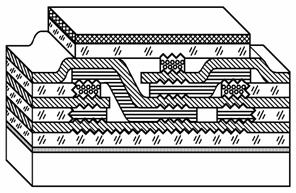
Figure 1. General view of a Design "Integrated Optical Logical Element"
In firm luminescent solids the intensity of luminescence depends on small quantities of impurity — activators. The complex combination of various processes is actually observed.
The radiation of the photoluminescence arises at absorption of only a certain lengths of waves by luminophor.
The use of the given technical decision opens the opportunity to transfer the existing level of computer facilities in optical area of a spectrum without using electronic components.
The development
contains "know-how". Developed at the Information Technologies
Department of Kherson National Technical University.
6.2 The Integrated Optical Generator of Pulses
The integrated optical generator of pulses allows to form a series of optical pulses with peak values of logic levels used in digital computer facilities [27].
The work of the integrated optical generator of pulses (fig. 2) is based on the use of physical properties of chemical compounds and their spectral characteristics.
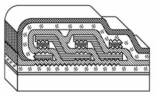
Figure 2. General views of a Design "Integrated Optical Generator of Pulses"
The generating part of the device consists of three logic elements of inversion. As a result of it the periodic pulses of identical duration are generated. The duration of periodic pulses will be equal
|
|
(10) |
where, ![]()
![]()
![]() — delay by the first, second and
third inverters accordingly. Taking into account such connection of logic
elements we receive a shift of fronts and a fall of pulses of one element
concerning another by value
— delay by the first, second and
third inverters accordingly. Taking into account such connection of logic
elements we receive a shift of fronts and a fall of pulses of one element
concerning another by value ![]() . It is known,
that their number should be odd but not less than three inverters. The application
of one inverter is inexpedient since the fronts and falls of pulses can not
achieve an optimum allowable level which will cause stochastic process.
. It is known,
that their number should be odd but not less than three inverters. The application
of one inverter is inexpedient since the fronts and falls of pulses can not
achieve an optimum allowable level which will cause stochastic process.
The use of the given technical decision, as specifying generator of the optical computer opens the opportunity to transfer the existing level of computer facilities in optical area of a spectrum without using electronic components.
The integrated optical generator of pulses can be used as a component of dynamic units of optical computing facilities.
The development contains "know-how". Developed at the Information Technologies Department of Kherson National Technical University.
6.3 The Integrated Optical Shaper of a
Single Pulse
The received device of the integrated optical shaper of a single pulse allows to form a short optical pulse in reply to the change of a logical level on an input with amplitude of logical levels accepted in digital computer facilities at the expense of the constructive decision using physical properties of chemical compounds and their wave parameters [28].
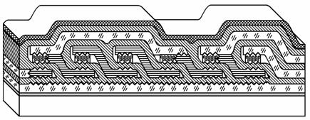
Figure 3. General views of a Design "Integrated Optical Shaper of a Single Pulse"
The integrated optical shaper of a single pulse (fig. 3) contains a source of basic radiation, phase gratings, optical waveguides, passive filters, active filters and photoactive elements.
With occurrence of a control signal on the input of optical waveguide the condition on input of the active filter changes. As the active filter is made active, it does not pass radiation from a source of basic radiation on an input of the photoactive element. By the elements of a delay the optical pulse is formed on an output.
The integrated optical shaper of a single pulse can be used as a component of dynamic units of optical computing facilities.
The development contains "know-how". Developed at the Information Technologies Department of Kherson National Technical University.
6.4 An Integrated Optical Multifunctional
Logical Element
The integrated optical multifunctional logical element is capable of forming optical channeling to carry out except for inversion and conjunction logical operations of a disjunction, logical functions: Pierce function "OR - INVERT", "AND - INVERT", operation of logical comparison, function sum on the module 2, arithmetic addition [29].
The work of an integrated optical multifunctional logic element is based on the use of physical properties of chemical compounds and their spectral characteristics.
The integrated optical multifunctional logic element (fig. 4) works as follows.
The analysis of conditions of distribution of optical radiation (basic and secondary) on optical system of the device in the absence of radiation on information inputs A and B (inputs of the second waveguide and the third waveguide accordingly) gives the following estimation of a condition of information outputs of the device: the secondary radiation takes place on the output C (output of the fourth waveguide), on the output D, on the output G, on the output H and on the output L. On outputs E, F and K the radiation is absent.
In feeding the secondary radiation on any
of information inputs of the device (A or B) the top part of
optical system from the third photoactive element and higher — remains
unchanged. It is due to the features of the second active filter which does not
pass radiation of a basic source of radiation on a branch ![]() through the first input to the
output, — if even on one of its inputs (second or third) there is a secondary
radiation from the first or the second photoactive elements. The exception
makes information outputs of the device of the first group C and D
on which the condition will change depending on the entrance conditions.
through the first input to the
output, — if even on one of its inputs (second or third) there is a secondary
radiation from the first or the second photoactive elements. The exception
makes information outputs of the device of the first group C and D
on which the condition will change depending on the entrance conditions.
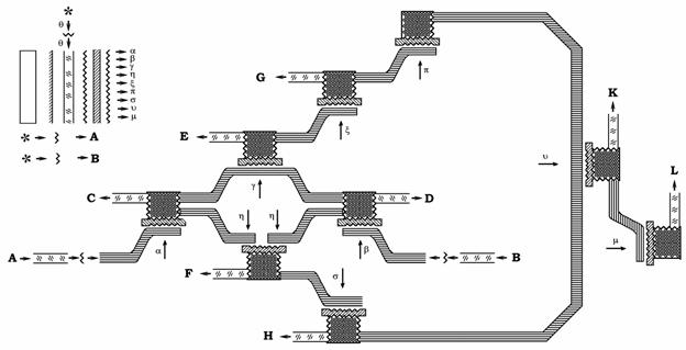
Figure 4. The Structural Circuit "Integrated Optical Multifunctional Logical Element"
The integrated optical multifunctional logic element is capable of performing seven logic operations with binary meanings of entrance variable and one arithmetic operation. The performance of operations is reflected by the truth table.
1. Logical inversion
|
|
(11) |
2. Logical conjunction
|
|
(12) |
3. Logical disjunction
|
|
(13) |
4. Logical operation "AND - INVERT"
|
|
(14) |
5. Logical Pierce function "OR - INVERT"
|
|
(15) |
6. Logical operation sum on the module 2
|
|
(16) |
7. Logical operation of comparison (equivalence)
|
|
(17) |
8. Arithmetic addition. In performing operation of addition of variables A and B as the result of addition will be the meaning on the output K with the use of carry in the senior bit at overflow from the output E:
|
|
(18) |

plus carry to the senior bit from E ![]()
The use of the given technical decision as a component of the optical processor gives the opportunity to transfer the existing level of computer facilities in optical area of a spectrum without using electronic components.
The integrated optical multifunctional logical element can be used as a component of the arithmetic logical device of the optical processor.
The development contains "know-how". Developed at the Information Technologies Department of Kherson National Technical University.
6.5 Integrated Optical Synchronized
RS-flip-flop
The integrated optical synchronized RS-flip-flop is capable of performing function of storing of logical conditions [30].
The work of integrated optical synchronized RS-flip-flop is based on the use of physical properties of chemical compounds and their spectral characteristics.
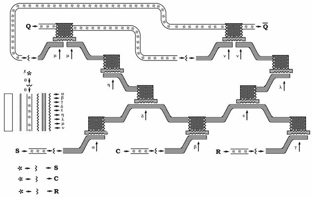
Figure 5. The Structural Circuit of "Integrated Optical Synchronized RS-Flip-Flop"
The characteristic equation of work "Integrated optical synchronized RS-flip-flop" (fig. 5) is submitted by the formula:
|
|
(19) |
It is supposed that before studying the
work of the flip-flop it was in the initial condition, i.e. the output ![]() is equal to logic zero
and the output
is equal to logic zero
and the output ![]() is
equal to logic unit. According to the classical theory the work of the
synchronized
is
equal to logic unit. According to the classical theory the work of the
synchronized ![]() flip-flop
can be checked up on the table of condition.
flip-flop
can be checked up on the table of condition.
Integrated optical synchronized RS-flip-flop works as follows. In
the initial condition the basic radiation passes on conditional branches from ![]() up to
up to ![]() from the source of
basic radiation through the first optical element of communication (OEC)
distributing on the first optical waveguide and passing through the second OEC
through the first passive filter, through the third OEC.
from the source of
basic radiation through the first optical element of communication (OEC)
distributing on the first optical waveguide and passing through the second OEC
through the first passive filter, through the third OEC.
Let's consider the situation in the absence of logical control
levels on inputs of the optical waveguides (![]() ), (
), (![]() ) and (
) and (![]() ), i.e. radiation of sources of the second
group and also on the second inputs of the first, the second and the third
active filters. As the active filters are not active they pass radiation freely
from the source of basic radiation on branches
), i.e. radiation of sources of the second
group and also on the second inputs of the first, the second and the third
active filters. As the active filters are not active they pass radiation freely
from the source of basic radiation on branches ![]() ,
, ![]() and
and ![]() to the first optical functional element
(OFE), to the fourth OFE and to the second OFE accordingly. The first, the
fourth and the second OFE comprise photoactive elements which exciting
irradiate the secondary radiation. Thereof the fifth and the fourth active
filters become active. Let us assume that the initial condition of the
considered flip-flop, — when on its inverse output
to the first optical functional element
(OFE), to the fourth OFE and to the second OFE accordingly. The first, the
fourth and the second OFE comprise photoactive elements which exciting
irradiate the secondary radiation. Thereof the fifth and the fourth active
filters become active. Let us assume that the initial condition of the
considered flip-flop, — when on its inverse output ![]() will be a logic unit, i.e. the
presence of the secondary radiation (due to the luminescence of the ninth OFE)
on the output of the fifth optical waveguide.
will be a logic unit, i.e. the
presence of the secondary radiation (due to the luminescence of the ninth OFE)
on the output of the fifth optical waveguide.
The change of the condition on inputs will result in change of the condition of components of the circuit.
The design offered allows to perform operations of storage of logical condition by optical channeling at the expense of physical properties of chemical compounds.
The use of the given technical decision as a component of the optical processor gives the opportunity to transfer the existing level of computer facilities in optical area of a specter without using electronic components.
Integrated optical synchronized RS-flip-flop can be used as a component of registers of the optical processor.
The development contains "know-how". Developed at the Information Technologies Department of Kherson National Technical University.
6.6 The Integrated Optical T-flip-flop
The integrated optical T-flip-flop allows to perform the function of the accounting flip-flop by using of physical properties of chemical compounds and their wave parameters, with this excluding the occurrence of the uncertain condition with the possibility to be applied for the construction of the accounting circuits appears [31].
The work of the integrated optical T-flip-flop (fig. 6-7) is based on the use of physical properties of chemical compounds and their spectral characteristics. By search of in common working optical components the decision on use of base basic radiation (in the given statement, — feeding all optical system) was accepted. As demonstration variant it is possible to take advantage of infra-red radiation as basic radiation.
Figure 6. The Structural Circuit "Integrated Optical T-Flip-Flop"
Figure 7. General view of a Design "Integrated Optical T-Flip-Flop"
Before considering the work of the
device it is necessary to note that the chosen structure of the T-flip-flop consists
of two parts. The first part is a unit of synchronization which consists of two
2-input elements And. The second part is proper asynchronous trigger consisting
of two 2-input elements OR - INVERT. Such configuration is chosen as base with
the purpose to reduce temporary delays influencing as a result speed (unlike
the circuits assembled from the same components). The T-flip-flop with one
information input T is represented by the asynchronous T-flip-flop which is
switched by the receipt the input T of a controlling signal as a logic unit.
The table of switchings of the T-flip-flop in the reduced form is submitted in
table 1 and in the complete form — in table 2.
|
Table 1 |
|
Table 2 |
|||
|
The Reduced Form of the Switchings of T-flip-flop |
|
The Complete Form of the Switchings of T-flip-flop |
|||
|
|
|
|
|
|
|
|
0 |
|
|
0 |
0 |
0 |
|
1 |
|
|
0 |
1 |
1 |
|
|
|
|
1 |
0 |
1 |
|
|
|
|
1 |
1 |
0 |
The characteristic equation of work "Integrated optical T-flip-flop" is submitted by the formula:
|
|
(20) |
It is supposed that before studying the
work of the flip-flop it was in an initial condition, i.e. the output ![]() is equal to logic zero,
and the output
is equal to logic zero,
and the output ![]() is
equal to logic unit.
is
equal to logic unit.
It is important to note that the installation of the flip-flop in
this or that condition should be accompanied by the controlling signal ![]() . And the control is
carried out by true logical meanings.
. And the control is
carried out by true logical meanings.
The change of a condition on a controlling clock input will result in change of the condition of components of the circuit.
At the moment of disappearance of the controlling signal ![]() the right branch
the right branch ![]() of feeding is
disconnected by basic radiation of the eighth element. But thus there remains a
left branch. As a result of it the flip-flop is in the condition of storage of
"unit" on the individual output
of feeding is
disconnected by basic radiation of the eighth element. But thus there remains a
left branch. As a result of it the flip-flop is in the condition of storage of
"unit" on the individual output ![]() .
.
Using the given technical decision as a component of the optical processor gives the opportunity to transfer the existing level of computer facilities in optical area of a spectrum without using electronic components.
The integrated optical T-flip-flop can be used as a component of counters of the optical processor.
The development contains "know-how". Developed at the Information Technologies Department of Kherson National Technical University.
6.7 The Integrated Optical D-flip-flop
The work of the integrated optical D-flip-flop is based on the use of physical properties of chemical compounds and their spectral characteristics [32].
The structural circuit "Integrated optical ![]() -flip-flop" is submitted in
figure 8. The general view of a design is submitted in figure 9.
-flip-flop" is submitted in
figure 8. The general view of a design is submitted in figure 9.
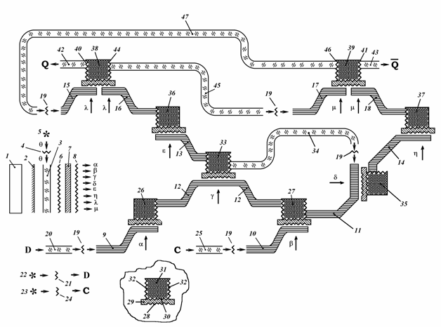
Figure 8. The Structural Circuit "Integrated Optical D-Flip-Flop"
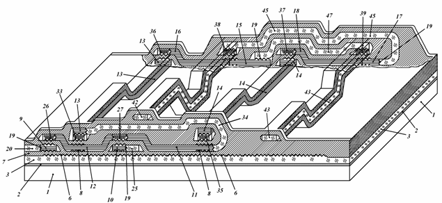
Figure 9. General view of a Design "Integrated Optical D-Flip-Flop"
Before considering the work of the device it is necessary to note
that the chosen structure of the ![]() -flip-flop consists of two parts. The first
part is a unit of synchronization which consists of two 2-input elements AND.
The second part is proper asynchronous trigger consisting two 2-input elements
OR - INVERT. Such configuration is chosen as base with the purpose to reduce
temporary delays influencing as a result speed (unlike the circuits assembled
from the same components) and realizes logic function
-flip-flop consists of two parts. The first
part is a unit of synchronization which consists of two 2-input elements AND.
The second part is proper asynchronous trigger consisting two 2-input elements
OR - INVERT. Such configuration is chosen as base with the purpose to reduce
temporary delays influencing as a result speed (unlike the circuits assembled
from the same components) and realizes logic function
|
|
(21) |
The characteristic equation of work "Integrated optical D-flip-flop" is submitted by the formula:
|
|
(22) |
It is supposed that before research of work of the flip-flop, it was
in an initial condition, i.e. the output ![]() is equal to logic zero, and output
is equal to logic zero, and output ![]() is equal to logic unit.
According to the classical theory the work of the
is equal to logic unit.
According to the classical theory the work of the ![]() flip-flop can be checked up by the table of
conditions (Table 3-4). The table of transitions of the D-flip-flop in the
reduced record is submitted in Table 3, and in the complete record — in Table
4.
flip-flop can be checked up by the table of
conditions (Table 3-4). The table of transitions of the D-flip-flop in the
reduced record is submitted in Table 3, and in the complete record — in Table
4.
|
Table 3 |
|
Table 4 |
||||
|
The Reduced Form of Transitions of the D-flip-flop |
|
The Complete Form of Transitions of the D-flip-flop |
||||
|
|
|
|
|
|
|
|
|
0 |
|
|
0 |
0 |
0 |
0 |
|
1 |
|
|
0 |
1 |
0 |
1 |
|
|
|
|
1 |
0 |
0 |
0 |
|
|
|
|
1 |
1 |
0 |
1 |
|
|
|
|
0 |
0 |
1 |
0 |
|
|
|
|
0 |
1 |
1 |
0 |
|
|
|
|
1 |
0 |
1 |
1 |
|
|
|
|
1 |
1 |
1 |
1 |
It is important to note, that the installation of the flip-flop in
this or that condition depends on meanings on the input D and
should be accompanied by clock ![]() . The change of conditions of the flip-flop
depends on the presence of clock on the input
. The change of conditions of the flip-flop
depends on the presence of clock on the input ![]() .
.
The integrated optical D-flip-flop works as follows.
In the initial condition the basic radiation passes on conditional
branches from ![]() up
to
up
to ![]() from a
source of basic radiation 5 through the first element 4, distributing on the
first optical waveguide 3 and passing through the second element 6, through the
first passive filter 7, through the third element 8.
from a
source of basic radiation 5 through the first element 4, distributing on the
first optical waveguide 3 and passing through the second element 6, through the
first passive filter 7, through the third element 8.
Let's consider a situation in the absence of logical controlled
levels on inputs of optical waveguide 20 (![]() ) and 25 (
) and 25 (![]() ), i.e. radiation from sources of radiation
of the second group 22 and 23, and also on the second inputs of the first of
the 9 and the second of 10 active filters. As active filters 9 and 10 are not
active they pass radiation freely from the source of basic radiation 5 (Fig. 8)
on branches
), i.e. radiation from sources of radiation
of the second group 22 and 23, and also on the second inputs of the first of
the 9 and the second of 10 active filters. As active filters 9 and 10 are not
active they pass radiation freely from the source of basic radiation 5 (Fig. 8)
on branches ![]() and
and
![]() . Let us
assume that the initial condition of the considered flip-flop, is that when on
its inverse output
. Let us
assume that the initial condition of the considered flip-flop, is that when on
its inverse output ![]() will
be logical unit, i.e. the presence of the secondary radiation on the output of
the fifth 43 optical waveguide.
will
be logical unit, i.e. the presence of the secondary radiation on the output of
the fifth 43 optical waveguide.
It is necessary to note, that the third 11 and the fourth 12 active filters are prototypes of elements of conjunction. It means that the specified active filters will pass basic radiation only in the case when on both of them (the second and the third) inputs there not is no activating radiation. If on one of the input of the active filter there is a secondary radiation, due to activization it will not pass through itself the basic radiation.
The occurrence of signals ![]() and
and ![]() on inputs of the second 20 and the eighth
25 optical waveguide will result in change of the logic condition of components
of the circuit.
on inputs of the second 20 and the eighth
25 optical waveguide will result in change of the logic condition of components
of the circuit.
It is necessary to note that the seventh 15 and the eighth 16 active filters and also the ninth 17 and the tenth 18 active filters, — represent a prototype of elements of disjunction.
The use of the given technical decision, as a component of the optical processor, gives the opportunity to transfer the existing level of computer facilities in optical area of a spectrum without using electronic components.
The integrated optical D-flip-flop can be used as a compound component of the registers of the optical processor.
The development contains "know-how". Developed at the Information Technologies Department of Kherson National Technical University.
7 Deductions
The technical decisions, submitted for discussion have advantages over all technical parameters with all existing ones now. These results should be perceived as one of the ways of the decision of the given technical task.
Conclusion
In many scientific bodies many perspective tasks are being solved. For the development of civilization one shouldn't miss the submitted opportunity given by the received result. As far back as 1881 A.Bell demonstrated his optical telephone. But the opinion of the authors his next design with the converter in an electrical signal was a mistake. If it had not taken place, the engineering would have developed improving optical communication lines. As a result it was at the end of XXth century when it occurred.
The important task of perfection of technical intellectual information systems is the search for methods and technological decisions. Using optimum ways for application of physical phenomena and their properties it is possible to specify categories of the development of element base of hardware of this millennium.
Gratitude
We would like to express our gratitude to Fomenko N.S., PhD (Phylology) for valuable comments on the language of the English variant of the article.
References
1. Moslehi B., Goodman J.W., Tur M., Shaw H.J. Fiber-Optic Lattice Signal Processing // Proc. of the IEEE, Vol. 72, N 7, pp. 909--930 (1984)
2. Verber C.M. Integrated-Optical Approaches to Numerical Optical Processing // Proc. of the IEEE, Vol. 72, N 7, pp. 942--953 (1984)
3. Ichioka Y., Tanida J. Optical Parallel Logic Gates using a Shadow-Casting System for Optical Digital Computing // Proc. of the IEEE, Vol. 72, N 7, pp. 787--801 (1984)
4. Vainovskis E. Elementārie un Kombinētie Loģiskie Elementi. // Pusvaditāju radioelektronika, lpp. 202-206. Zvaigzne, Rigā (1985)
5. А. с. USSR № 575603, Int. cl.-2 — G 02 F 3/00, Publ. October 05.1977, Rep. № 37.
6. United States Patent N 3,941,455. U.S. Cl. 350/160 LC; 340/173 LT; 250/213 R; 332/7.51. Int. Cl.2. G11 C 11/42; G02 F 1/13. Publ. Mar. 2, 1976.
7. Voronin E.S., Divlekeyev M.I., Ilyinskij Yu.A., Solomatin V.S. Preobrazovaniye izobrazheniya iz infrakrasnogo diapazona v vidimyj metodami nelineynoy optiki. // ZhETF, T. 58, № 1. S. 51--59 (1970)
8. Korenyeva L.G., Zolin V.F., Davydov B.L. Nelineynaya optika molekularnyh kristallov, 200 s. Nauka, Moskwa (1985)
9. Organicheskiye fotohromy. Pod red. prof. A.V.Yeltsova, 288 s. Khimiya, Leningrad (1982)
10. Entcyklopediya neorganicheskih materialov, T. 2, S. 394--398. Glavnaya redaktsiya ukrainskoy sovetskoy entcyklopedii, Kiyev (1977)
11. Entcyklopediya neorganicheskih materialov, T. 1, S. 720--723. Glavnaya redaktsiya ukrainskoy sovetskoy entcyklopedii, Kiyev (1977)
12. Gutorov M.M. Osnovy svetotehniki i istochniki sveta. 2-ye izd, 384 s. Energoatomizdat, Moskva (1983)
13. Barachevckij V.A., Lashkov G.I., Tsehomskij V.A. Fotohromizm i yego primeneniye, S. 31--57. Khimiya, Moskva (1977)
14. Photochromism. Techn. Chem., v. 111. Ed. G.H.Brown, P. 633. Wiley-Interscience, New York (1971)
15 Arkhangelskaya V.A, Kiselyova M.N., Feofilov P.P. A. c. SSSR № 265317, MKI-2 — G 02 B 1/02. // Otkrytiya. Izobr. Prom. obraztsy. Tovarn. znaki, N 33, S. 223 (1971)
16. Feofilov P.P. "Optika i spektroskopiya", T. 12. S. 531--533 (1962)
17. Arkhangelskaya V.A., Feofilov P.P. Proc. Intern. Conf. on Luminescence, pp. 1682--1688 (1966)
18. Arkhangelskaya V.A, Kiselyova M.N. // Spektroskopiya kristallov, S. 164--167. Nauka, Moskva (1970)
19. Arkhangelskaya V.A, Kiselyova M.N., Shrayber V.M. // Fizika tvyordogo tela, T. II, S. 869--876 (1969)
20. Cohen A.J., Smith H.L. "Science", V. 137, P. 981 (1962)
21. Cohen A.J. VII-th Internal Congress on Glasses, V. 2, pp. 111.1--111.9. Brussels (1965)
22. Swarts E.L., Pressau J.P. J. Amer. Ceram. Soc., v. 48, pp. 333--338 (1965)
23. Patent USA, N 3664725, Nat. Cl. 350--160 (1972).
24. Nizovtsev V.V. i dr. // Zhurnal prikladnoy spektroskopii, T. 18, S. 333--335 (1973)
25. Meiling G. Phys. a. Chem. Glasses, V. 14, pp. 118--121 (1973)
26. Pylypenko M.V., Gnydets V.P., Hodakov V.Yeg., Doshchenko G.G., Tsivilsky F.N., Glukhova V.I. The Declaration Patent of Ukraine N 67083 A, The Integrated Optical Logic Element. Int.Pat.Cl.-7 G02F3/00, G02B6/12, Publ. June 15 2004, Rep.N 6. / Assignee: Kherson National Technical University (2004)
27. Pylypenko M.V., Hodakov V.Yeg., Shekhovtsov A.V., Tsivilsky F.N., Polyakov V.S., Petrikov Ig.F. The Declaration Patent of Ukraine for useful model N 12957, The Integral Optical Generator of Pulses. Int.Pat.Cl.-(2006) H03K3/027-(2006.01), G02F3/00, Publ. March 15 2006, Rep.N 3. / Assignee: Kherson National Technical University (2006)
28. Pylypenko M.V., Hodakov V.Yeg., Shekhovtsov A.V., Tsivilsky F.N., Polyakov V.S., Petrikov A.F. The Declaration Patent of Ukraine for useful model N 13526, The Integral Optical Shaper of a Single Pulse. Int.Pat.Cl.-(2006) H03K5/14, G02F3/00, Publ. April 17 2006, Rep.N 4. / Assignee: Kherson National Technical University (2006)
29. Pylypenko M.V., Hodakov V.Yeg., Shekhovtsov A.V., Tsivilsky F.N., Shaganyan S.N., Kobylyakov D.A. Patent of Ukraine for useful model N 18222, Integral Optical Multifunctional Logic Element. Int. Pat. Cl (2006) G 02 F3/00, G 06 E1/00, G 02 B5/00, G 02 B6/12. Publ. November 15 2006, Rep. N 11. / Assignee: Kherson National Technical University (2006)
30. Pylypenko M.V., Hodakov V.Yeg., Shekhovtsov A.V., Tsivilsky F.N., Baranenko R.V., Kozel V.N., Drozdova Ye.A. The Declaration Patent of Ukraine for useful model N 14957, The Integral Optical Synchronized RS-Trigger. Int.Pat.Cl.-(2006) G02F3/00, G02B5/20, G02B6/12, H03K3/037 (2006.01), Publ. June 15 2006, Rep.N 6. / Assignee: Kherson National Technical University (2006)
31. Pylypenko M.V., Hodakov V.Yeg., Tsivilsky F.N., Kiriychuk D.L., Bozhko S.L. Patent of Ukraine for useful model N 23696, The Integral Optical T-Trigger. Int.Pat.Cl.-(2006) G02F3/00, G02B5/22, G02B6/12, G06E1/00, H03K3/037 (2007.01), H03K19/02, Publ. June 11 2007, Rep.N 8. / Assignee: Kherson National Technical University (2007)
32. Pylypenko M.V., Hodakov V.Yeg., Tsivilsky F.N., Grigorova A.A., Bozhko S.L., Kiriychuk D.L. Patent of Ukraine for useful model N 24198, The Integral Optical D-Trigger. Int.Pat.Cl.-(2006) G02F3/00, G02B5/22, G02B6/12, G06E1/00, H03K3/037 (2007.01), H03K19/00, Publ. June 25 2007, Rep.N 9. / Assignee: Kherson National Technical University (2007)