|
“ЖУРНАЛ РАДИОЭЛЕКТРОНИКИ” N 8, 2009 |
(C-V) and Y-Parameters Determination of JFETs under Different Environmental Conditions
S. M. El-Ghanam
Women’s College
for Arts, Science, and Education,
Ain shams University, Heliopolis, Cairo Egypt
Received July 17, 2009
The C-V characteristics of n-channel JFET have been measured as a function of temperature up to 140 0C and γ- rays up to 100 kGy. The results show that the input capacitance Ciss is an increasing function of temperature when measured at small bias voltage and low frequency bands. On the other hand, Ciss was shown to decrease from 11.68 down to 8.17 nF due to γ- exposure up to 100 kGy. In addition, the physical parameters of the gate-source junction were investigated, where their values were to shown to be funcion of both temperature increasing and γ- exposure. The values of the Y- parameters of common-source amplifier were calculated under influence of temperature and γ- rays. The result shows that, the susceptance component of the admittance increases due to temperature increasing, while decreasing after γ- exposure. The investigation was extended to include the temperature and radiation effects on the cutoff frequency fT0 . It is clear from calculations that, as the temperature increases from 30 0C up to 140 0C, fT0 dropped from 47 MHz down to 5 MHz, at 0.8 Volt. On the other hand its value was shown to increase from 43 MHz up to 102 MHz, at 0.8 Volt, due to γ- exposure up to 100 kGy.
Keywords: JFET, input capacitance , Y-parameters , quality factor, dissiption factor, phase angle, impedance, cutoff frequency.
Определение (C-V) и Y-параметров полевого транзистора с управляющим p-n переходом при различных условиях окружающей среды
С. М. Эл-Ханам
Университет Каира, Египет
Получена 17 июля 2009 г.
Были измерены вольтамперные характеристики n-канального полевого транзистора как функции температуры до 140 градусов и гамма-облучения до 100 kGy. Резуьтаты показывают, что входная емкость растет с температурой при измерении с малым напряжением смещения и в низкой полосе частот. С другой стороны, показано, что Ciss уменьнается от 11.68 до 8.17 nF при гамма-облучении до 100 kGy. Также были исследованы физические характеристики перехода затвор-исток, которые оказались зависящими от повышения температуры и от гамма-облучения. Были рассчитаны зависимости значений Y-параметров усилителя с общим истоком от температуры и гамма-облучения. Оказалось, что реактивная часть адмитанса увеличивается при увеличении температуры и уменьшается при гамма-облучении. Было также исследовано влияние температуры и радиации на частоту отсечки fT0. Из вычислений следует, что при росте температуры от 300C до 1400C fT0 падает с 47 MHz до 5 MHz при 0.8 V. С другой стороны, ее значение .увеличивается с 43 MHz до 102 MHz при 0.8 V благодаря гамма-облучению до 100 kGy
.Ключевые слова: полевой транзистор, входная емкость, Y- параметр, коэффициент потерь, фазовый угол, импеданс, частота отсечки
1.Introduction:
Capacitance – Voltage (C-V) measurements provide an excellent means of monitoring the formation of channels on junction field effect transistors [1-3]. On the other hand, admittance or y – parameters are widely used to describe the characteristics of electronic devices, where the values of the y – parameters for junction field effect transistor (JFET) are affected by the internal capacitance values [4]. The physical structure of the JFET produces inter- terminal capacitances; these are the gate-drain capacitance Cgd , the gate-source capacitance Cgs , and the drain source capacitance Cds.
In data sheet these are represented by Ciss (input), Coss (output), and Crss (reverse transfer) capacitances, where [5]:
Ciss = Cgs + Cgd
Coss = Cds
Crss = Cgd
In determining the switching performance of a JFET device Ciss is the most important factor. When an input voltage pulse is applied to a device, the input capacitance must be charged and discharged, before VGS come rise, or fall to its final value. The common-source FET amplifier is affected by the interelectrode capacitance that affects its high – frequency performance. On the other hand, the mutual conductance of a FET will fall at high frequencies. The intrinsic cut–off frequency fT0 of JFET is the frequency at which transconductance gm0 has fallen to 0.7 times its value at 1kHz. Also, fT0 is depending on Cgs and Cgd [6-8]. Therefore this paper is concerned with studying the inter- terminal capacitances of N- channel JFET, wherever the devices are operated under different environmental conditions such as temperature or γ- ray exposure. Also, the paper was extended to include the influence of temperature and radiation on y- parameters, and intrinsic cut-off frequency.
2. Experimental Procedure:
The temperature dependence of C-V relationship and common source y-parameters of N-channel Junction Field Effect Transistors (JFET) of type 245B are investigated in the temperature range from 10 0C up to 140 0C. In addition, gamma- radiation effects were also studied when JFET devices were exposed up to 100 kGy. The gamma source used is a Cobalt -60, and irradiation process was carried out at the National Center for Radiation Research and Technology, Atomic Energy Authority of Egypt. A programmable automatic RCL meter, model PM 6306, manufactured by Fluke was used for precise measurements of C-V and C-F characteristics of the proposed devices. Finally, using the obtained results the following physical parameters are investigated:
1- Gate-to-source capacitance; Cgs .
2- Drain-to-source capacitance; Cgd .
3- Quality factor; Q-factor.
4- Dissipation factor; D-factor.
5- Phase angle; φ.
6- Impedance; R.
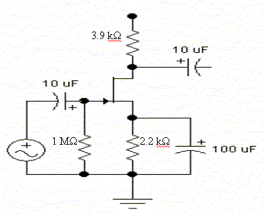
Also, the paper was extended to include the study of the common source Y-parameters of N-JFET amplifier circuit shown in Fig.( 1 ) when operated at different elevated temperature levels (from 10 0C up to 140 0C ), and also before and after γ-exposure up to 100 kGy.
Fig. (1) JFET amplifier circuit.
3. Results and Discussion:
In the present paper, an attempt was carried out in order to shed further light on some physical and electrical characteristics of JFET devices. In this concern the C-V and C-F characteristics, common- source Y-parameters, and calculated intrinsic cut off frequency (fT0 ) of JFET were studied under the influence of temperature and γ- radiation.
3.1 C-V Characteristics:
For studying the reverse gate –source and gate- drain junctions the C-V relationships were plotted at a reverse bias voltage ranging from 0.0 to 5 Volt at steps of 0.1 Volt, at different frequency levels in the range from 100 Hz up to 1 MHz .
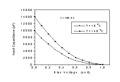
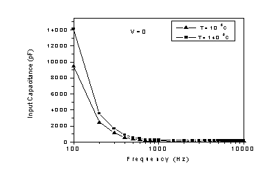
Figures (2a and 2b) show C-V and C-F curves of the input capacitance plotted at two temperature levels of 10 0C and 140 0C. It is clear that the input capacitance value is a direct function of both voltage and frequency values. As well, it is clear from the same figures that the input capacitance is a function of temperature when measured at small bias voltage and low frequency bands. From which, Fig. (2c) shows that, the input capacitance increases with temperature in the range from 10 0C up to 140 0C, measured at 100 Hz and 1MHz.
Fig. (2a) (Ciss – bias voltage) relationship measured at two temperature levels.
Fig. (2b) (Ciss – F ) relationship measured at two temperature levels.
Fig.(2c) Temperature dependence of input capacitance of JFETs
measured at different frequency levels.
Figures 3(a and b) show Ciss plotted as a function of bias voltage (Fig. 3a) and frequency (Fig. 3b) before and after exposure to gamma dose levels of 50 kGy and 100 kGy. At zero bias voltage, and frequency of 100Hz (Fig.3a), an initial value of Ciss was measured to be 11600 pF. This value was shown to decrease down to 8100 pF due to γ- exposure up to 100 kGy. On the other hand, and at higher bias voltage values, the change in capacitance value due to γ- exposure is shown to be less sensitive. Also, at higher frequency values the change in Ciss due to γ- exposure is negligible.
Fig.(3a) Gamma-irradiation effects on (Ciss – bias voltage ) curves of
JFETs.
Fig.(3b) ( Ciss – F ) relationship measured before and after exposure to
different gamma-ray doses.
The obtained decrease in the capacitance value, measured at same bias voltage, may be attributed to a widening occurs at the edges of the space charge region for the same applied voltage. On other words, due to the formation of a very narrow intrinsic region in the neighborhood of the metallurgical PN – junction, i.e., compensation of the chemical doping by radiation induced deep traps will tend to produce a region [9-11].
3.2 Temperature effect on physical parameters of gate- source junction:
By definition, the quality factor of a junction (Q) can be expressed as the ratio of the inductive reactance of the junction to its resistance. On the other hand, the dissipation factor (D)is governed by the equation
D = 1/ 2π FCR
The temperature effect on both Q- and D- factors was investigated in the range from 20 0C up to 140 0C. It is clear from Fig. (4) that on reverse gate- source mode the increasing of temperature leads to a pronounced decrease in quality factor and increase in dissipation factor.
Fig. (4) Temperature effects on quality- and dissipation- factors for the gate-source junction of the tested transistor.
Also, the investigation was extended to include the temperature effects on the impedance and phase angle (Fig.5). Considering the junction impedance, it is clearly shown, from Fig. (5), that the gate-source junction impedance is greatly affected by temperature variations. The junction impedance was shown to decrease from an initial value of 430 Ω, measured at 20 0C, down to 200 Ω, measured at 120 0C.` Also, it is clear from the same figure that the phase angle decreases with temperature increase, where, its value decreased from -37, measured at 20 0C down to -42, measured at 140 0C.
Fig. (5) Variation of gate-source junction impedance and phase angle as a function of temperature for JFETs.
3.3 Radiation Effect on Physical Parameters of Gate- Source Junction:
The Q- and D- factors were measured at different reverse gate-source bias voltage values before and after exposure to tow gamma dose levels of 50 kGy and 100 kGy. Figure (6) shows that the Q-factor was decreased due to γ- exposure where the rate of decrease is a function of bias voltage. As an example, a Q- value of 11.2, measured at VGS =1 volt, was decreased down to 7.2 due to γ- exposure up to100 kGy. While at bias voltage value of 0.4 it is clear that the shift in the Q-factor due to gamma irradiation is negligible. On the other hand, it is clear from the same figure that the dissipation factor was shown to increase due to gamma exposure, where at 0.4 volt, an initial D-factor value of 2.5 was shown to increase up to 5 due to gamma exposure up to 100 kGy. But for higher bias voltage values (1.0 Volt), the D-factor was shown to be less sensitive to gamma irradiation.
`
Fig. (6) Bias voltage dependence of quality- and dissipation- factors for the gate-source junction before and after gamma exposure up to 100 kGy.
Considering the impedance and phase angle, Fig. (7) shows their dependence on gate-source voltage, measured before and after gamma- ray exposure to two different dose levels of 50 kGy and 100 kGy. It is clearly shown that the impedance was insensitive to γ- exposure for bias voltage values up to 0.6 volt. But for higher bias voltage values, the effect of gamma- rays is shown to cause a slight decrease on the impedance value, where an initial value of 1455 kΩ, measured at 1.0 Volt, decays to 1259 kΩ due to gamma-dose up to 100 kGy. On the other hand, the phase angle was shown to increase on the same rate all over the bias voltage range.
Fig. (7) Variation of gate-source junction impedance an phase angle as a function of bias voltage for JFET before and after gamma exposure up to 100 kGy .
3.4 Y-parameters of Common Source JFET Amplifier:
The values of the y-parameters of JFET are quoted at specific frequency, often in terms of a real and an imaginary part that represent the conductance and susceptance components, as:
Forward transfer admittance yfs = gfs + jbfs = gm - jωCgd
Output admittance yos = gos + jbos = 1/ rd + jω (Cgd + Cds)
Input admittance yis = jbis = jω (Cgs + Cgd)
Reverse transfer admittance yrs = jbrs = -jωCgd
Where gm is the transconductance and, rd is ac drain resistance.
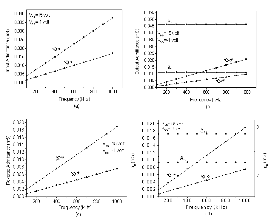
3.4.1 Temperature Effects on Common Source Y- parameters:
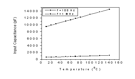
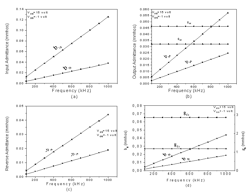
The proposed device was connected as a common- source amplifier with bias voltages VDS and VGS values of 15 volts and -1 volt, respectively (Fig.1). The capacitances Cgs, Cgd and Cds were measured in the frequency range from 1kHz up to 1MHz at different temperature levels up to 140 0C. From which, the components values of Y- parameters were calculated. Figure (8) shows the Y- parameters as a function of signal frequency plotted at two temperature levels of 30 0C and 140 0C. It is clear from this figure that the obtained values of Y-parameters are greatly affected by temperature variations, where the input admittance (Fig. 8a) increases by more than four orders of magnitude due to increasing of temperature up to 140 0C, calculated at 1MHz. On the other hand, Fig.(8b) shows that the susceptance component of the output admittance (bos) increased due to increasing temperature, while gos decreased, the matter which is due to the increase in dynamic resistance values with increasing temperature level. Also, the susceptance component of forward and reverse admittance values increase with increasing of the temperature up to 140 0C, but gfs value was shown to decrease .
Fig.(8) Temperature effects on common-source admittances versus
frequency ( ■ T= 30 0C, ▲T= 140 0C ).
3.4.2 Radiation effects on common- source Y- parameters:
The effect of γ- radiation on common- source admittance values have been investegated. The frequency dependence of capacitances Cgs, Cgd and Cds were measured and the values of admittance were calculated and plotted before and after γ- exposure up to 100 kGy (Fig. 9). From which it is quite observed that all the device admittances are a decreasing functions of γ- exposure up to 100 kGy.
Also, it is clear that the effect of radiation on the input and reverse admittances was much higher, wherever the devices operate at high frequency levels (Fig.9a,9c). The conductance components of the output and forward admittances were shown to be more sensitive to irradiation, where the reduction in gos and gfs values are shown in Fig. 9b,9d.
The large decrease in admittances value due to γ- exposure is mainly attributed to the reduction of inter- terminal capacitances, transconductance and ac resistance of JFET due to γ- exposure[12,13] .
Fig.(9) common-source admittances versus frequency before and after gamma exposure
( ■ before irradiation, ▲ Dose= 100 kGy ).
3.5 Investigation of Intrinsic Cutoff Frequency under Influence of Temperature and γ- Radiation:
The cutoff frequency fT0 was calculated for JFETs using DC measurement results applying the following equation [14]:
fT0 = gm0 /2π (Cgs+ Cgd )
Since gm0, Cgs, and Cgd are all functions of temperature, then the dependence of fT0 on temperature can be easily obtained.
Fig.(10) Cutoff frequency versus bias voltage calculated at different temperature levels.
Figure (10) shows the dependence of fT0 on the voltage bias calculated at different temperature levels. It is clear that for bias voltage values less than 0.4 Volt, the temperature effect is shown to be insignificant. But for higher bias voltage value, fT0 dropped from 47 MHz down to 5 MHz, measured at bias voltage of 0.8 Volt due to temperature increase, where as an example fT0 dropped from 47 MHz, measured at 30 0C and 0.8 Volt. Down to 5 MHz (measured at 140 0C and 0.8 Volt ).
Finally, fT0 was calculated before and after γ- exposure (Fig.11). It is clear that fT0 value increase after γ- exposure up to 100 kGy.
Fig.(11) Cutoff frequency versus bias voltage calculated before and after gamma exposure up to 100 kGy.
Conclusion:
From the experimental results, analysis, and discussions, it could be concluded that operation of JFET devices at different elevated temperature levels, or exposed to γ- radiation, a pronounced changes on the C-V characteristics, physical parameters of gate- source junction, common- source Y- parameters, and cutoff frequency are noticed. The results show that the input capacitance is a function of temperature and γ- radiation when measured at small bias voltage and low frequency bands. Also, the Y-parameters are greatly affected by temperature and γ- exposure. Finally the temperature and γ- radiation effects on fT0 is significant at higher bias voltage values.
References:
1- D. C. Green, "Electronics II ", England, 1988.
2- D.P. Norton, "Capacitance-Voltage Measurements on Ultrathin Gate Dielectric", Solid State Electronics, Great Britain, pp. 801- 805, May 2003.
3- F.A.S. Soliman, "Operation of Bipolar and Field Effect Transistors in Radiation Environments", Commun. Fac. Sci. Univ., Ankara, Vol. 43, pp. 9-23, 1995.
4- Yung- Lung Hsu., et al., "Modeling of Abnormal Capacitance- Voltage Characteristics Observed in MOS Transistor with Ultra- Thin Gate Oxide", Solid State Electronics, Great Britain, pp. 1941-1943, November 2002.
5- T.F. Bogart, "Electronic Devices and Circuits", New Jersey, 1997.
6- J.I. Izpura," Side Contact Effects on the Capacitance Properties of Junction Devices", Semiconductor Science and Technology, pp. 243-249, April 2001.
7- S. Altindal, et al., "The Role of Interface State and Series Resistance on the I-V and C-V Characteristics in AL/SnO2/p-Si Schottky Diodes", Solid State Electronics, Great Britain, Vol. 47, pp. 1847-1854, 2003.
8- Jae-Ki Lee, "Temperature Dependence of DTMOS Transistor Characteristics", Solid State Electronics, Great Britain, Vol. 48, pp. 183-187, 2004.
9- F.A.S. Soliman, et al., "Characteristics and Radiation Effects of MOS Capacitors with AL2 O3 Layers in p-Type Silicon", Appl. Radiat. Isot., Great Britain, Vol. 46, No. 5, pp. 355-361, 1995.
10- F.A.S. Soliman, et al., "Effects of Electron-Hole Generation, Transport and Trapping in MOSFETs Due to γ-Ray Exposure", Appl. Radiat. Isot., Great Britain, Vol. 46, No. 12, pp. 1337-1343, 1995.
11- G.F.D. Betta, "Effects of /SPL Gamma/-Rays on JFET Devices and Circuits Fabricated in a Detector-Compatible ", IEEE Trans. Action, on Nucl. Sci.,Vol. 50, Issue 6, pp. 2474-2480, 2003.
12- S.M. El-Ghanam, "Temperature and Radiation Effects on the Characteristics of N-Channel JFETs", A.M.S.E., France, Modelling A, Vol. 77, No. 2, pp. 73-85, 2004.
13- J. Assaf, "High gamma dose induced damage on two types of discrete JFET transistors", Physica B, Vol. 404, pp. 73–78, 2009.
14- Lei Zhany, et al. "Fabrication and Charcterization of Ga N Junction Field Effect Transistors", Material Research Society, Boston, F99W4.9, 1999.