DESIGN OF T-SPLIT POWER DIVIDERS USING DUMBBELL SHAPED DGS
1Tamasi Moyra, 2Susanta Kumar Parui, 2Santanu Das
1Department of Electronics and Communication Engineering,
National Institute of Technology, Agartala
2Department of Electronics and Telecommunication Engineering,
Bengal Engineering and Science University, Shibpur,
Howrah – 711 103, INDIA
Received August 3, 2012
Abstract. Power dividers and power
combiners are passive microwave components for power dividing and power
combining. In this paper attention has been given towards the implementation of
equal power divider using conventional 50![]() microstrip
line and dumbbell shaped defected ground structures (DGS). DGS increase the
effective inductance and capacitance of the line, supporting slow-wave
propagation. Thus, it increases the effective line impedance of the microstrip
line. Consequently, all passive and active components that are implemented
using DGS have a miniaturized size compared to conventional components. In this
paper one 3 dB or equal power divider has been implemented at 1.2 GHz in the
first step. In the next part of the paper, one unequal power divider of
dividing ratio 2:1 has been designed using DGS with microstrip line. Those dividers have wide
applications in microwave circuits and feeds of array antennas.
microstrip
line and dumbbell shaped defected ground structures (DGS). DGS increase the
effective inductance and capacitance of the line, supporting slow-wave
propagation. Thus, it increases the effective line impedance of the microstrip
line. Consequently, all passive and active components that are implemented
using DGS have a miniaturized size compared to conventional components. In this
paper one 3 dB or equal power divider has been implemented at 1.2 GHz in the
first step. In the next part of the paper, one unequal power divider of
dividing ratio 2:1 has been designed using DGS with microstrip line. Those dividers have wide
applications in microwave circuits and feeds of array antennas.
Keywords: microstrip, defected ground structure, equal power divider, unequal power divider.
Аннотация. Предложена и исследована конструкция микрополоскового симметричного (3дБ) и несимметричного (2:1) делителя мощности. Для согласования делителей используется отверстие в подложке в форме гантели. Неоднородность увеличивает эквивалентную индуктивность и улучшает согласование.
Ключевые слова: микрополосковая линия, неоднородная подложка, симметричный делитель мощности, несимметричный делитель мощности.
I. INTRODUCTION
Power dividers are passive microwave circuits. They are often of the equal-division (3 dB) type, but unequal power division ratios are also possible [1-2]. T-split power divider is a simple three port network that can be used for power division or power combining which can be implemented in virtually any type of transmission line medium [3]. It can be made to be matched at all ports for equal-split or unequal power division ratios.
This device is also potentially lossless as no reflected power from output ports enters into it. This divider has wide applications in microwave circuits and antenna feeds, but it has a narrow bandwidth, which has the best performance at a center frequency.
Defected Ground Structure (DGS) is the etched pattern of particular shape in the ground plane of microstrip line or CPW structure. DGSs affect the parameters of circuit that can be expressed as: making interference in the fields of ground plane, increasing permittivity, increasing effective inductance and capacitance properties in transmission lines, increasing effective characteristic impedance of the transmission line, providing a bandstop characteristic and supporting slow wave propagation [4-10].
In this paper, it is proposed to improve the effective line impedance with reduction in size and dimensions of the T-split power divider by the application of DGSs. Utilizing the feature of DGS one equal or 3dB power divider has been designed at the operating frequency of 1.2 GHz. Then the output divided powers are again divided equally in different levels. In the last step one 2:1 unequal power divider has been designed using the proper DGS structure.
II.PARAMETRIC STUDY AND EFFECT ON CHARACTERESTIC IMPEDANCE OF DGS
The dumbbell shaped DGS underneath a conventional microstrip line is shown in fig 1(a). The characteristic response of DGS provides one stop band characteristic due to the introducing of some inductance and capacitance by DGS as shown in fig 1(b). The head of the dumbbell is responsible for introducing some inductance ‘L’, transverse slot connecting the dumbbell heads is responsible for introducing some capacitance ‘C’. Thus, the DGS structure can be represented by L-C equivalent circuit as 1st order elliptical bandstop filter as shown in Fig. 1(c). Therefore, implementation of DGS with microstrip line also changes the characteristic impedance of microstrip line.
|
|
|
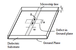
The structure is fabricated with FR4 substrate with dielectric constant 4.4, substrate height h = 1.58mm and negligible loss tangent.
Let, the
different dimensions of the above structure are W = 3mm for 50![]() microstrip line, DGS head length a = 5mm
with width 4mm and two heads are connected by a transverse slot of length 4mm
and width g = 0.4mm.
microstrip line, DGS head length a = 5mm
with width 4mm and two heads are connected by a transverse slot of length 4mm
and width g = 0.4mm.
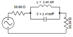
Fig. 1 (c). Equivalent Circuit
The equivalent L and C values can be obtained using the expressions as follows:
 (1)
(1)
 (2)
(2)
Where, f0
and fc are attenuation pole and attenuation zero
frequencies respectively and Z0 = 50![]() is
the characteristic impedance of the microstrip line.
is
the characteristic impedance of the microstrip line.
Thus, the obtained values of inductance, L=2.46 nH and C=2.47095 fF of the taken DGS structure.
The etching of the defect on the ground plane, increases the path of the
ground currents, thus increases the inductance per unit length,![]() . Increase in
. Increase in ![]() results
in the increase of the line impedance. However, the effect of
results
in the increase of the line impedance. However, the effect of ![]() also has to be considered. The capacitance
can be claimed to be decreased since the distance between the ground and the
signal line has increased. In the standard microstrip line, the fields are
confined between the line and the ground, at the distance ruled by the
thickness of the substrate, but when the defect is placed beneath the line, the
fields confined between the ground and the line are inclined, resulting in an
increased distance; hence a lower capacitance. The low capacitance is another
factor which increases the line impedance. So, the effect of both
also has to be considered. The capacitance
can be claimed to be decreased since the distance between the ground and the
signal line has increased. In the standard microstrip line, the fields are
confined between the line and the ground, at the distance ruled by the
thickness of the substrate, but when the defect is placed beneath the line, the
fields confined between the ground and the line are inclined, resulting in an
increased distance; hence a lower capacitance. The low capacitance is another
factor which increases the line impedance. So, the effect of both ![]() and
and ![]() causes
the line impedance to increase.
causes
the line impedance to increase.
The effective line impedance can be represented by
 (3)
(3)
The variation of the different parameters with the variation of dumbbell head area by the variation of head length, ‘a’ keeping other parameters constant is shown in the following Table: 1.
Table 1. The variation of the different parameters with ‘a’(with
line impedance 50 ![]() )
)
|
Length, ‘a’ (mm)
|
Inductance ‘L’ (nH)
|
Capacitance ‘C’ (pF) |
Line
impedance ‘Zline’ (
|
|
2 |
1.529 |
2.54065 |
62.327 |
|
4 |
2.143 |
2.46834 |
72.73 |
|
5 |
2.46 |
2.47095 |
77.965 |
|
6 |
2.774 |
2.4295 |
82.094 |
Thus, the effect of DGS which is responsible for providing high impedance line can be explained in the above way.
The variation of inductance, capacitance and effective line impedance with the dumbbell head length ‘a’ as represented in table 1 are shown graphically in Fig. 2.
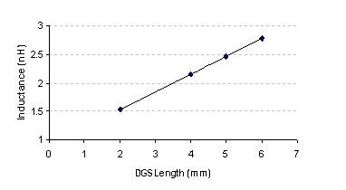
Fig. 2(a). Variation of inductance with length ‘a’
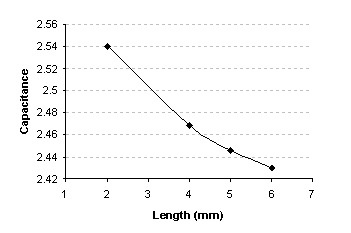
Fig. 2(b). Variation of capacitance with length ‘a’
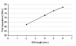
Fig. 2(c). Variation of effective line impedance with length ‘a’
III. DESIGN PROCEDURE OF EQUAL SPLIT POWER DIVIDER
(a) 3-dB or Half power divider:
By definition, a 3 dB power divider is an ideally passive, lossless, and
reciprocal three port device that divides power equally in magnitude with equal
output phase [3]. From the general study as, one 3 dB (equal split) power
divider can be made by using a 50![]() input line and two 100
input line and two 100![]() output lines [3]. In this paper, the 50
output lines [3]. In this paper, the 50![]() input line has been constructed using
conventional microstrip line and two 100
input line has been constructed using
conventional microstrip line and two 100![]() output
lines are implemented using dumbbell shaped DGS underneath a conventional 50
output
lines are implemented using dumbbell shaped DGS underneath a conventional 50![]() microstrip line.
microstrip line.
From the
analysis of the curve (Fig. 2(c)), mathematically with the help of curve
fitting it can be found that the rectangular headed proposed DGS of head
length, a = 9.48 mm is required to obtain the effective line impedance of 100![]() .Therefore, here one dumbbell shape DGS
with two rectangular heads of length 9.48 mm and width 5mm connected with a
transverse slot of length 4mm and width 0.4mm underneath a 50
.Therefore, here one dumbbell shape DGS
with two rectangular heads of length 9.48 mm and width 5mm connected with a
transverse slot of length 4mm and width 0.4mm underneath a 50![]() microstrip line is used to obtain 100
microstrip line is used to obtain 100![]() output lines. Each 100
output lines. Each 100![]() line can be represented by equivalent
lumped elements of inductance, L = 4.442 nH and capacitance, C = 438.8 fF.
line can be represented by equivalent
lumped elements of inductance, L = 4.442 nH and capacitance, C = 438.8 fF.
The schematic diagram of the proposed 3dB or equal power divider is shown in the following Figure 3(a) and the characteristic response is shown in the Figure 3(b) .
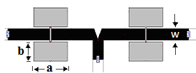
Fig. 3(a). Proposed 3dB or equal power divider
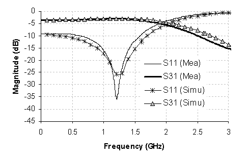
Fig. 3(b). Scattering parameters
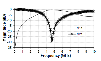
The 3dB power divider is implemented at center frequency 1.2 GHz and fabricated with FR4 substrate. The above simulated response shows that the input power (applied at port 1) is equally divided between two output ports (port 2 and port 3) and the value of output power is 3dB up to 2 GHz. The photonic view of the proposed structure is shown in the following Fig 4.
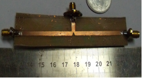
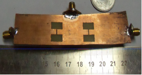
(a) (b)
Fig.4 Photonic View (a) Top plane, (b) Ground plane
The simulated and measurement responses are shown Fig. 4(c) and Fig. 4(d)
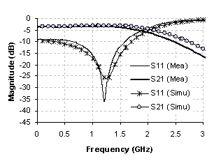
Figure 4(c) S-parameters (simulated and measured) S11 & S21
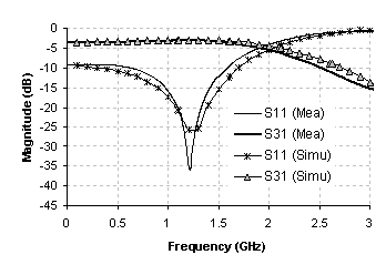
Figure 4(d) S-parameters (simulated and measured) S11 & S31
From the above responses it has been obtained that the proposed structure provides 3dB coupling at the operating frequency 1.2 GHz and there is a good agreement between the simulated and measurement responses.
IV. DESIGN OF 2:1 POWER DIVIDER USING DGS
In this section attention has been given towards the design of one unequal power divider of dividing ratio 2:1 at the output port using the same concept of design of equal power divider.
(a) Calculation of output port impedances:
Fig. 5 shows
the simple T- junction power divider structure. The T-junction power divider can be
modeled as a junction of three transmission lines [3], as follows:
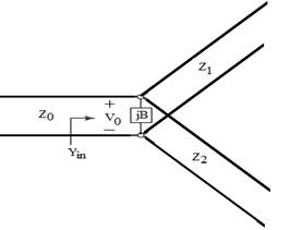
Fig 5. Transmission line model of a
lossless T-junction
If the voltage at the junction is V0, as shown in the Fig. 5, the output power to the matched divider is
 (4)
(4)
while, the output powers are
 (5)
(5)
 (6)
(6)
these results yield the characteristic impedances as

then the input impedance to the junction is
![]()
So, that the input is
matched to the 50![]() source.
source.
(b) Design Procedure :
75![]() line can be obtained with the help of
microstrip line of width 1.4 mm and length 28mm through which two-third of the
total input power will be passed.
line can be obtained with the help of
microstrip line of width 1.4 mm and length 28mm through which two-third of the
total input power will be passed.
The other
output line i.e. 150![]() line can be obtained by
Dumbbell shaped Diffective Ground structure (DGS) underneath 75
line can be obtained by
Dumbbell shaped Diffective Ground structure (DGS) underneath 75![]() microstrip line. The variations of
different parameters with the variation of the DGS head width keeping other
parameters are tabulated in table 2:
microstrip line. The variations of
different parameters with the variation of the DGS head width keeping other
parameters are tabulated in table 2:
Table: 2 The variation of the different parameters with ‘b’(with
line impedance 75 ![]() )
)
|
Rectangle Head width (mm) |
Resonance freq, f0 (GHz) |
3dB stop band (GHz) |
Inductance L(nH) |
Capacitance C (fF) |
Line impedance, Zc ( |
|
5.0 |
3.60 |
3.34 |
6.153 |
317.7 |
139.2 |
|
5.5 |
3.51 |
3.80 |
7.406 |
279.2 |
162.87 |
|
6.0 |
3.35 |
3.93 |
8.362 |
269.9 |
176 |
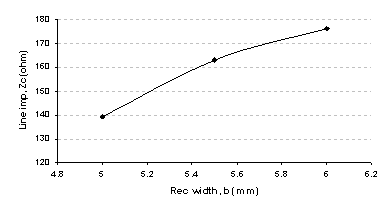
Fig. 6. Variation of effective line impedance with head width
Mathematically, with the curve fitting of the above response, it can be found that the rectangular width, ‘b’, and effective microstrip line impedance, ‘Zc’, related with each other by the following equation:
y = 0.0005x2 - 0.1181x + 11.665 (7)
Therefore, the
obtained value of the rectangular width, ‘b’ for the 150![]() line
will be 5.2mm.
line
will be 5.2mm.
The proposed
structure of the 2:1 unequal power divider is shown in the following Fig. 7(a)
and the characteristic responses are shown in the Fig. 7(b). The circuit has
been designed with FR4 substrate. The different dimensions are a = 10mm, b
=5.2mm and two heads are connected by 4mm long, 0.4mm width transverse slot.
The width of 50![]() microstrip line is W = 3mm and
that of 75
microstrip line is W = 3mm and
that of 75![]() microstrip line is W1 = 1.4mm.
microstrip line is W1 = 1.4mm.
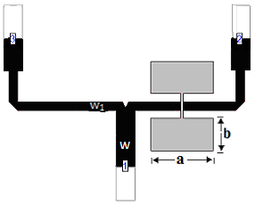
Figure 7(a) 2:1 Power Divider using DGS
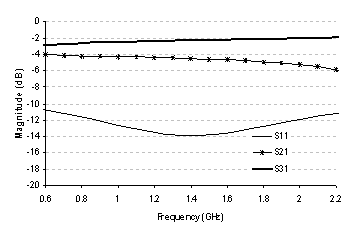
Figure 7(b) Scattering Parameters
The above structure shows that the transmitted power at 1.2 is almost 4.1 dB and that of at port 3 is almost 2 dB i.e the input power divided in 2:1 ratio at port 2 and port 3. Thus, the proposed structure acts as a 2:1 power divider.
V. Conclusion
In this paper
one important property of the DGS i.e. increment of the characteristic
impedance of the transmission line compare to the conventional one has been
used to design equal or unequal power divider. The characteristic impedance of
the output line must be too high to design power divider. Design of high
impedance line can be possible utilizing very narrow width transmission line
but practically fabrication of that narrow width is almost impossible.
Therefore, the high impedance line can be easily achieved with conventional
microstrip line along with DGS. One 100![]() line
is designed with conventional 50
line
is designed with conventional 50![]() microstrip line which
is required to design equal or 3 dB power divider. Similarly, one 150
microstrip line which
is required to design equal or 3 dB power divider. Similarly, one 150![]() line can be achieved with 75
line can be achieved with 75![]() microstrip line addition with DGS which
is required for designing of unequal 2:1 power divider.
microstrip line addition with DGS which
is required for designing of unequal 2:1 power divider.
Acknowledgment
The work is funded by CSIR, New Delhi, Govt. of India.
References
[1] J.-S. Lim, S.-W. Lee, C.-S. Kim, J.-S. Park, D. Ahn, and S. Nam, "A 4:1 Unequal Wilkinson Power Divider," IEEE Microwave and Wireless Components Letters, Vol. 11, no. 3, pp. 124 - 126, Mar. 2001.
[2] Chang, C.-P., C.-C. Su, S.-H. Hung, Y.-H. Wang, and J.-H. Chen, "A 6 : 1 unequal wilkinson power divider with EBG CPW," Progress In Electromagnetics Research Letters, Vol. 8, pp. 151-159, 2009.
[3] D. M. Pozar, Microwave Engineering, 3rd ed. Hoboken, NJ: John Wiley & Sons, 2005.
[4] Scardelletti, M. C., G. E. Ponchak, and T. M. Weller, “Miniaturized wilkinson power divider utilizing capacitive loading,” IEEE Microwave and Wireless Components Letters, Vol. 12, No. 1, 6–8, Jan. 2002.
[5] Shamsinejad, S., M. Soleimani, and N. Komjani, “Novel miniaturized wilkinson power divider for 3g mobile receivers,”Progress In Electromagnetics Research Letters, Vol. 3, 9–16, 2008.
[6] Papapolymerou1, J., G. E. Ponchak, and E. M. Tentzeris, “A wilkinson power divider on a low resistivity Si substrate with a polyimide interface layer for wireless circuits,” IEEE MTTS International Microwave Symposium Diqest, Vol. 1, 593–596, Jun. 2002.
[7] Sung, Y. J., C. A. Ahn, and Y. S. Kim, “Size reduction and harmonic suppression of rat-race hybrid coupler using defected ground structure,” IEEE Microwave and Wireless Components Letter, Vol. 14, No. 1, 7–9 Jun. 2004.
[8] J. S. Lim, H. S. Kim, J. S. Park, D. Ahn, and S. Nam, “A power amplifier with efficiency improved using defected ground structure,” IEEE Microwave Wireless Component. Letter., Vol. 11, pp. 170–172, Apr. 2001.
[9] J. S. Lim, J. S. Park, Y. T. Lee, D. Ahn, and S. Nam, “Application of defected ground structure in reducing the size of amplifiers,” IEEE Microwave Wireless Compon Lett., Vol. 12, pp. 261–263, July 2002.
[10] J.-S. Lim, C.-S. Kim, J.-S. Park, D. Ahn, and S. Nam, "Design of 10dB 900 branch line coupler using microstrip line with defected ground structure," IEEE Electronics Letters, vol. 36, no. 21, pp. 1784 1785, Oct. 2000.