Determination of technological parameters of drift transistors according to specified operational characteristics
A.N.
Frolov1, К.A. Frolov1,
S.V.
Shutov2
1- Kherson National State University, 2- Institute of Semiconductor Physics by V. Lashkaryov
NASU
Received February 18, 2008
Algorithm of determination of physical parameters of a transistor structure for obtaining a specified set of its basic electrical characteristics has been presented. Empirical formulas derived by statistic processing of a large quantity of experimental data which allow to determine parameters of structure of drift n-p-n-transistor with the most optimum combination of output characteristics have been used for building the algorithm.
Existing methods and computation algorithms of bipolar transistors both discrete as well as bipolar chip elements assume carrying out of calculation of electric parameters and characteristics of transistors on the basis of known modes of the basic technological operations in the following sequence: known technology - parameters of impurity distribution - electric parameters and characteristics. However, during real designing of transistors - either the best foreign analogs or as the elements of microchips – its electric parameters and characteristics are known or given, and technology regarding the modes of technological operations represents "know-how". In that case a usage of known methods and algorithms of computation demands searching a great number of variants of modes of technological operations to obtain a demanded set of parameters and characteristics. It demands significant expenditures of time even using computer facilities as well as very high qualification of the developer, based on large practical experience and developed intuition. But even under these conditions the set of electric parameters and characteristics of transistors often is not optimal for the chosen variant of technology.
It is known, that drift transistors have the best set of parameters, but its calculation is more difficult and longer, than for diffusion transistors.
With the purpose of reduction of time for development of drift transistors and bipolar microchips as well as for obtaining of optimal set of parameters and characteristics of transistors it is necessary to apply the calculation method in the following sequence: electric parameters and characteristics - parameters of impurity distribution - modes of technological operations.
The investigations carried out (including the present work) allow to offer following computation algorithm of drift n - p - n transistors using new method:
The task for carrying out of the calculations includes:
- minimum amplification coefficient - BNmin;
- maximum amplification coefficient - BNmax;
- emitter-base breakdown voltage Vebo;
- collector-base breakdown voltage Vcbo;
- collector-emitter breakdown voltage Vceo;
- the mode for the measurement of parameters – Vk and Ik (collector voltage and current).
Parameters of impurity distribution in the drift transistor are:
- impurity concentration at the emitter-base p-n-junction Neb;
- impurity concentration at the collector-base p-n-junction Ncb;
- emitter depth (emitter-base p-n-junction depth) Xje;
- base depth (collector-base p-n-junction depth) Xjb;
- thickness of high-resistance collector Wc;
The calculation of impurity distribution parameters consists of three steps:
- calculation of parameters of collector-base junction (Ncb, Xjb) and concentration Neb;
- calculation of additional values;
- computation of base thickness Wbo, emitter depth Xje and thickness of high-resistance collector Wk.
Computation algorithm on the first step includes:
- calculation of the coefficient showing the difference of diffusion p-n-junction from the abrupt one by avalanche breakdown voltage χF [1]
χF = 1+3.6 . 10-4 (Vebo)2.54 ;
- calculation of impurity concentration at the emitter-base junction [2]
Neb =
;
- calculation of the avalanche breakdown voltage of the collector-base p-n-junction Vcbo.a [3]:
Vcbo.a. = Vceо .
;
- calculation of specific resistance of an epitaxial layer ρep [4]:
- rounding of value ρep to the magnitude corresponding to technical specification for epitaxial structures and assignment of ρep for further calculations in the interactive mode;
- calculation of breakdown voltage of the flat area of p-n-junction Vbr.fl. [5]:
Vbr.fl. = 86 .
0.64 ;
- calculation of impurity concentration at the collector-base p-n-junction Ncb [6]:
Ncb =
;
- calculation of base region depth Xjb (the depth of collector-base junction) [4]
Xjb = 0.144
;
- rounding of the obtained value Xjb and adding to it a margin of 0.1÷0.3 μm (for the usage in technical documentation and further calculations in the interactive mode).
Computation algorithm on the second step includes:
- calculation of contact potential difference at collector and emitter junctions [7]:
;
;
- calculation of carrier mobility next to emitter (by Neb) and collector p-n-junctions [8]:
,
;
- calculation of diffusion coefficient next to emitter and collector p-n-junction Dne, Dnc, Dpe, Dpc [7]:
D =
;
- calculation of the life time τne, τpe, τnc, τpc [9]:

- calculation of carrier diffusion length Lne, Lpe, Lnc, Lpc (
) [5].
Computation algorithm on the third step includes:
- calculation of averaged impurity concentration in base Nb.av. [10]:
;
- calculation of minimum base thickness Wb.min [10]:
;
- calculation of maximum base thickness Wb.max [11]:
;
- calculation of average base thickness Wb.av.:
;
- rounding the value of technological thickness of base Wb.av, taking it for further calculations and putting it into technical documentation Wbo (in the interactive mode);
- calculation of emitter depth
;
- calculation of high-resistance collector thickness [12]:
.
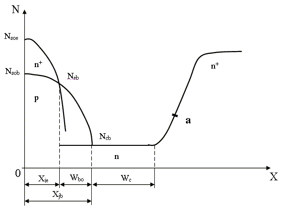
Thus, the parameters of impurity distribution Ncb, Neb, Xje, Xjb, Wk are determined in the process of calculations.
The method offered for calculation of impurity distribution parameters in the drift n-p-n transistor allows to determine an impurity distribution in the base region and to estimate the thickness of a high-resistance collector Wc with sufficient degree of accuracy.
However, a real breakdown by overlapping which determines breakdown voltage Vcbo does not occur when the depth of space-charge region (SCR) of a collector-base junction becomes equal to the thickness Wc, but when SCR reaches some point A (fig.1) being in the region of diffusion of an n+-hidden layer (for bipolar microchips).
Fig.1. Impurity distribution in the drift n-p-n transistor.
Up to the present time there is no technique of the accurate enough determination of the overlap voltage by the impurity distribution in the regions of n+-layer diffusion, though this is an actual problem for both transistors as well as diodes. The absence of such a technique affects especially strongly devices of SHF range as well as high-power devices.
An excess distance in the region of high-resistance collector leads to occurrence of an additional resistance which reduces working frequency and results in a saturation voltage that conducts to excess dissipated power in the device, to the overheat and reliability degradation. Thus the problems of obtaining of preset diffusion of layers in the technological process, calculation of impurity distribution in it as well as calculation of the overlap voltage in the region of diffusion are still actual.
References:
1. Samoilov N.A., Frolov A.N., Shutov S.V. Breakdown voltages of p-n-junctions in planar transistors // St. Petersburg journal of electronics. 1999, № 1, pp.44-46.
2. Samoilov N. A., Frolov A. N., Shutov S. V. Operational estimate of the impurity concentration in the emitter in designing n-p-n drift transistors.- Technical Physics Letters, Volume 22, № 4, 1996, pp.281-282.
3. Grebene A.B. Project engineering of analog integrated circuits. Moscow, Energiya. 1976. 435 p.
4. Frolov, A. N., Shutov, S. V. Quick estimation of the resistivity of collector and the depth of the collector junction in the design of bipolar n-p-n transistors // Technical Physics, 1998, Volume 43, № 8 , pp. 1005-1006.
5. Trutko A.F. Methods of transistors calculation. Moscow: Energiya, 1971, 272p.
6. Samoilov N.A., Frolov A.N., Shutov S.V. Technique of express estimation of breakdown voltage of n-p-n transistors // St. Petersburg journal of electronics. 1996, № 4, pp.42-45.
7. Vikulin I.M., Stafeyev V.I. Physics of semiconductor devices. Moscow, Sov.radio. 1980. 296p.
8. Maller R., Keymins T. Elements of integrated circuits. Moscow, Mir. 1989. 630p.
9. Gave K.I.S. / Solid St. Electronics / V.8. № 12. P.991-99.
10. Maronchuk I.E., Frolov, A. N., Shutov, S. V. Determination of the base thickness of a drift transistor by "punch-through" voltage. - Radio electronics and communications systems, 2001, vol. 44; part 11, pages 46-49.
11. Frolov A.N., Shutov S.V., Shershen’ A.M. Estimation of base thickness of drift n-p-n transistor through its amplification coefficient. Radioelektronika. 2001. № 12, pp.53-56.
12. Fedotov Ya.A. Silicon planar transistors. Moscow, Sov.radio. 1973. 336p.