Hot-electron superconducting nanobolometers-sensors and arrays of
them for high sensitive Terahertz frequency range imaging radiometers
V. A. Cherepenin, A. N. Vystavkin,
A. G. Kovalenko, S. V Shitov, O. V. Koryukin, I. A. Cohn,
A. A. Kuzmin, A. V. Uvarov, A. S. Il’in
Kotel’nikov Institute of Radioengineering and Electronics of RAS
Received March 22, 2011
Abstract. The comparative review of investigations and development state of super high sensitive superconducting nanobolometers-sensors for terahertz frequency range imaging array radiometers is presented. The conclusion concerning preferred design of such bolometers is made. Hot-electron nanobolometers with combined radiation absorber and transition edge sensor (TES) are most promising for the achievement of utmost high sensitivity as opposed to bolometers which radiation absorbers are made as suspended membranes and transition edge sensors are just membrane temperature measuring elements. Dimensions of absorber-TES combination have to be small to the limit – down to tens of nanometer, and operation temperature has to be super low – down to 30 – 40 mK. The networks of immersion lens, planar antenna, microstrip and coplanar lines with nanobolometer coupled into them have to be used to match THz radiation energy transfer to such small nanobolometers. The design, fabrication technology and application of imaging radiometers using mentioned above nanobolometers-sensors are considered.
Keywords: terahertz detector arrays, utmost high sensitivity, imaging radiometers.
Аннотация. Представлен сопоставительный обзор состояния исследований и разработок сверхчувствительных сверхпроводниковых наноболометров-сенсоров для матричных изображающих радиометров терагерцового диапазона частот. Сделан вывод о предпочтительной конструкции таких болометров. Наиболее обещающими с точки зрения достижения максимально высокой предельной чувствительности являются наноболометры на горячих электронах с сенсором на краю сверхпроводникового перехода (СКП = TES), совмещенным с поглотителем излучения, в противоположность болометрам, у которых поглотителем излучения являются подвешенные мембраны, а сенсоры на краю сверхпроводникового перехода являются элементами, измеряющими температуру мембран. Размеры совмещенного поглотителя-СКП должны быть предельно малыми: вплоть до нескольких десятков нанометров, а рабочая температура должна быть сверхнизкой: вплоть до 30 – 40 мК. Для согласования при передаче энергии терагерцового излучения к таким малоразмерным наноболометрам должны быть применены интегральные блоки, состоящие из иммерсионных линз, планарных антенн и микрополосковых и копланарных линий с включенными в них наноболометрами. Рассмотрены конструкция, технология изготовления и применения изображающих радиометров с названными выше наноболометрами-сенсорами.
Ключевые слова: матрицы терагерцовых детекторов, предельно высокая чувствительность, изображающие радиометры.
1. Nanobolometers. At the present time the electromagnetic oscillations of transitional (between millimeter and far infrared ranges) frequency range f = 0.3 – 10 THz (λ = 1 mm – 30 μm) and the corresponding detector devices find applications in several spheres: astronomical observations of farthest galaxies, development and application of security systems, apparatus for medical diagnostics, environment monitoring devices, various production control procedures including staple foods and so on. Nanobolometers based on the very low temperature superconducting nanostructures being in transition state are very important for the listed above applications. Why nanobolometers? The well known quasiparticle Cooper pair [1] has acquired recently one more name – “nanoparticle”. Fig. 1 explains this.
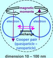
Fig. 1. The Cooper pair – nanoparticle.
When this nanoparticles are
occurring in a thin film structure of nanometer thickness: a single layer of
superconductor or in a two-layer “superconductor - normal metal”
structure – the very important physical properties reveal
themselves: dimension effect in the superconducting single layer structure and
proximity effect in the two-layer “superconductor - normal metal”
structure [1]. Characteristic thicknesses of thin films in both cases are 10 –100
nm order what is commensurable with dimension of nanoparticle “Cooper pair”. Both named above
effects result in possibility to adjust an operating temperature of
nanobolometer by force of the adjustment of layers thicknesses to operation temperature of
cryorefrigerator which cools nanobolometer. The
next substantial argument – the dependence
of the noise equivalent power of nanobolometer on temperature T and
absorber volume v of nanobolometer as ![]() [2]. As we have seen the
thickness is enough small (10 – 100 nm). The transversal dimensions have to be
as small as possible as well. The available fabrication technology being in our disposal provides
dimensions up to ~ 1 μm × 100 nm.
[2]. As we have seen the
thickness is enough small (10 – 100 nm). The transversal dimensions have to be
as small as possible as well. The available fabrication technology being in our disposal provides
dimensions up to ~ 1 μm × 100 nm.
2. Nanostructure effects. Experiments on said above nanostructure effects study are described in this section.
2.1. The dimensional effect in the single thin film superconducting structure. The dimensional effect occurs in the single thin film superconducting structure at very low temperatures. The effect is a partial suppression of superconductivity on the score of short distance (10 – 30 nm) between thin film boundaries. The partial suppression intensifies significantly the boundaries influence on interaction of paired electrons what reduces superconductivity transition temperature. We have studied [3] this effect in superconducting titanium thin film (Fig. 2). The superconductivity transition temperature was reduced from ~ 387 to ~ 297 mK, i. e. for ~ 23 % as it is necessary to match this temperature with operation temperature of 3He sorption cryorefrigerator.
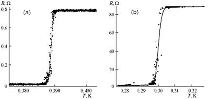
Fig. 2. The dimensional effect in superconducting titanium thin film structure; films thickness: (a) 320 nm, (b) 30 nm [3].
2.2. The proximity effect in two-layer thin film structure “superconductor - normal metal”. We have described this effect earlier [4] but repeat description briefly here for generality. This effect is the mutual partial penetration for nanometer distances of Cooper pairs from superconductor to normal metal and normal electrons in opposite direction [5]. These displacements result in the partial suppression of superconductivity in two-layer thin film structure. The possibility of the reducing the superconductivity transition temperature Tc in two-layer thin film structure “molybdenum – copper” was studied in the laboratory of authors together with P. L. Kapitza Institute of Physical Problems of RAS [4] in respect of TES-nanobolometers (Table 1 and Fig. 3). Sample I is of single-layer molybdenum. It is given here as initial one to demonstrate the critical temperature lowering due to proximity effect.
Table 1
|
Sample |
Thicknesses of layers, nm |
Critical temperature Tc, K
|
Normal resistance RN, Ohm |
R(T) characteristic slope
|
Operation bias U, V |
Noise equivalent power estimation NEP,W/Hz1/2 |
|
|
Mo |
Cu |
||||||
|
I |
12 |
0 |
0,93 |
67 |
1070 |
- |
- |
|
II |
15 |
35 |
0,40 |
2,9 |
150 |
10-7 |
~ 4·10-19 |
|
III |
12 |
35 |
0,27 |
2,6 |
320 |
10-8 |
~ 4·10-20 |
|
IV |
12 |
100 |
0,08 |
0,6 |
510 |
10-9 |
~ 4·10-21 |
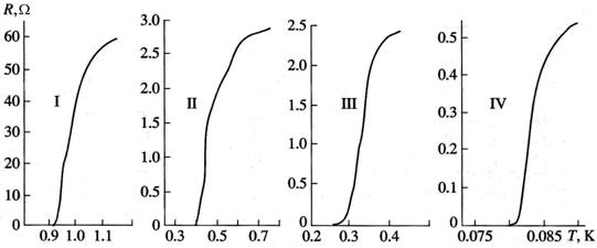
Fig. 3. The proximity effect in two-layer thin film structure “molybdenum – copper”; explanation in the text.
In both cases (at Fig. 2 and Fig 3) transverse dimensions of samples are l × w = 15 × 1.5 mm2. The NEP estimations for nanobolometers which can be fabricated of this structures with mentioned above R(T) characteristics and thicknesses were performed for samples transverse dimensions reduced to 1.5 × 0.15 μm2. The estimations were performed on the basis of the measured R(T) dependences and the electron energy balance equation [4, 6] like that as in other similar works [7]. The estimation results for Mo/Cu structures are represented in Table 1 and results for Mo/Cu and for Ti structures are shown at comparative plot of Fig. 8.
3. Two ways of the designing receiving arrays with nanobolometers. Two types of TES-nanobolometers[1]) are under consideration: (a) suspended at membranes or spider-webs [8] and (b) coupled to antennas [2]. Examples are given at Fig. 4. Membranes 1 (there are seven of them in the given example [8]) are mounted into frame using legs 1. The THz radiation in this case is provided to each membrane using horns 3 with resonance section behind membrane to improve radiation absorption. Two bandpass filters at 77 K and 4 K cut excess thermal radiation off.
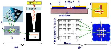
Fig. 4. Receiving arrays based on nanobolometers-sensors and radiation concentrated horns and planar antennas, explanation in text.
The attached to each membrane TES 4 is carrying out thermometer function. The thermometer readings correspond to the radiation power absorbed by membrane. In case of nanobolometers coupled to antennas [2] the radiation absorber and TES in each nanobolometer are combined (Fig. 4, position 5). The reaction mass absorbing radiation is the electron gas in the absorber-sensor. In this case the electron gas is heated by radiation and its temperature is increasing in comparison with absorber-sensor film. By this reason nanobolometers under consideration have definition “hot-electron”. The design example of such nanobolometer and the antenna providing it with THz radiation power are shown at Fig. 4,b as well (positions 5 - 8) [9]. Properly nanobolometer with combined absorber-sensor, more precisely absorber-TES, in this case is the single superconducting thin film or two-layer thin film structure “superconductor-normal metal” (Fig. 4,b, position 5). In this design a perpendicularly crossed two double-slot planar antennas are employed what makes possible to receive independently radiation power of both polarizations. The array of such nanobolometers 8 is formed by the integration of single nanobolometers as this is shown at Fig. 4,b and Fig. 5 (on the right) or by the integration in camomile form shown at Fig. 5 (on the left) as well. The radiation can be provided to set of planar antennas by horns (Fig. 4,a) or by immersion lenses. Two possible immersion lens array configurations are shown at Fig. 5. The structure of planar antennas and immersion lenses combination shown at Fig. 4,b and Fig. 5 provides the realization of hot-electron TES-nanobolometers with micron/submicron transverse dimensions what is necessary for the obtaining utmost high noise equivalent power for unique astrophysical observations.
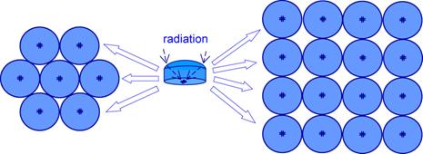
Fig. 5. The arrays of receiving elements with immersion lenses for THz radiation reception.
4. Fabrication of THz integrated receiving microcircuits. The combination of electron beam and optical lithography processes is accepted as main concept for fabrication THz integrated receiving microcircuits. The electron beam lithography is destined for fabrication of THz absorbers-sensors and matching elements having micron/submicron transverse dimensions while the optical lithography is destined for fabrication of other components and parts of receiving microcircuits. In the capacity of example the microphotograph of the fabricated THz integrated receiving microcircuit with single polarized double-slot antenna matched with nanobolometer-sensor by microstrip and coplanar line sections is shown at Fig. 6. The network composed of transverse micron sized 10 × 1 μm2 titanium absorber-sensor of 30 nm thickness in the middle (main component of nanobolometer-sensor) with microstrip and coplanar line sections on the left and right of it corresponds to the lower level of the integrated receiving microcircuit. It has twin niobium electrodes at the ends. Its draft is given below at Fig. 6 for clarity. The absorber-sensor is placed in the middle of network between massive niobium electrodes providing the hot electrons Andreev reflection from them [10]. The whole network is fabricated using electron beam lithography process. The top layer of niobium coated with gold to prevent THz radiation losses forms area with double slots of antenna and slots the edges of which are opposite electrodes of coplanar lines. The latter form short-circuit quarter wavelength sections for the blocking THz radiation. The center slot with coplanar line is excited by double slot antenna, and the coplanar line transmits THz energy to absorber-sensor. The middle isolating layer of integrated receiving microcircuit (transparent) is of SiO2.
One may expect the NEP ≈ 10-19 W/Hz1/2 of such integrated receiving microcircuits at operation temperature ≈ 0.3 K as well as NEP ≈ 10-20 W/Hz1/2 and better with transverse dimensions 1 × 0,1 μm2 and operation temperature ≈ 30 – 40 mK. The results of these estimations are made in section 2 and presented at Fig. 8. The latter sensitivity is needed for most advanced space projects SPIRIT [11], FIRI [12], MILLIMETRON [13] and others.
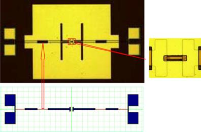
Fig. 6. The microphotograph of the fabricated THz integrated receiving microcircuit, explanation in text.
Fig. 7. Temperature dependences of two Ti
absorber microbridges in the vicinity of a litle bit less than 0.3 K, dimensions
of microbridges are l × w × t![]() 100 × 10 × 0.03 μm3.
100 × 10 × 0.03 μm3.
The first R(T) measurment results of two micrometer-sized combined absorbers-sensors fabricated using electron beam lithography process are shown at Fig. 7. The mentioned above estimation of value of NEP ≈ 10-19 W/Hz1/2 at
reduced samples transverse dimensions to 1 × 0.1 μm2 and at temperature ≈ 0.3 K for samples with R(T) shown at Fig. 7 were performed using the method briefly described in section 2. We have to take notice that dimensions l and w of measured microbridge samples is 15000 times larger each (Fig. 2 and Fig. 3) and 100 times larger each (Fig. 7), correspondingly, in comparison with model microbridge sample transverse dimensions of 1 × 0.1 μm2 chosen for estimations. In spite of such difference in transverse dimensions of experimentally measured samples the resulting estimated NEP’s are almost the same what is a posteriory evidence of the identity of samples physical properties at different transverse dimensions as well as the estimation calculations methodology correctness.
5. The comparison of
TES-nanobolometer NEP’s. We have carried out the
comparison of TES-nanobolometer NEP’s on the basis of Ti and Mo-Cu
samples estimated in section 2 with analogous values obtained by other authors.
The comparison results are presented at the plot of Fig. 9. The best NEP at the plot measured optically using
radiation at frequency 0.35 THz (λ ![]() 850 μm) is ~ 3·10-17 W/Hz1/2.
This figure is related to radiometer SCUBA-1 containing 34 × 40
nanobolometer array installed at J. C. Maxwell telescope [14].
Nanobolometers are attached to membranes of transverse dimensions ~ λ × λ, the radiation
is concentrated onto membranes using horns analogous to that what are shown at
Fig. 4,b. These nanobolometers are operated at temperature ~ 100 mK. Almost
similar optical NEP
850 μm) is ~ 3·10-17 W/Hz1/2.
This figure is related to radiometer SCUBA-1 containing 34 × 40
nanobolometer array installed at J. C. Maxwell telescope [14].
Nanobolometers are attached to membranes of transverse dimensions ~ λ × λ, the radiation
is concentrated onto membranes using horns analogous to that what are shown at
Fig. 4,b. These nanobolometers are operated at temperature ~ 100 mK. Almost
similar optical NEP![]() 10-16 W/Hz1/2 at the same
wavelength but in cryorefrigerator with operating temperature ~ 0.3 K is
obtained in [8]. The design of these nanobolometers is shown at Fig. 4,a. In both
cases absorbers of nanobolometers are rather large by area (~ λ × λ) what causes their large
volume v, i.e. sufficiently larger
than absorbers of nanobolometers coupled to antennas (Fig. 4,b). This causes considerably larger (the worse)
values of NEP
in comparison with expected ones at volumes of TES-nanobolometers with
micron/submicron transverse dimensions of absorber-sensors coupled to antennas.
Data on NEP’s at the plot of Fig. 9 are borrowed from works the
references on what are given at the plot.
10-16 W/Hz1/2 at the same
wavelength but in cryorefrigerator with operating temperature ~ 0.3 K is
obtained in [8]. The design of these nanobolometers is shown at Fig. 4,a. In both
cases absorbers of nanobolometers are rather large by area (~ λ × λ) what causes their large
volume v, i.e. sufficiently larger
than absorbers of nanobolometers coupled to antennas (Fig. 4,b). This causes considerably larger (the worse)
values of NEP
in comparison with expected ones at volumes of TES-nanobolometers with
micron/submicron transverse dimensions of absorber-sensors coupled to antennas.
Data on NEP’s at the plot of Fig. 9 are borrowed from works the
references on what are given at the plot.
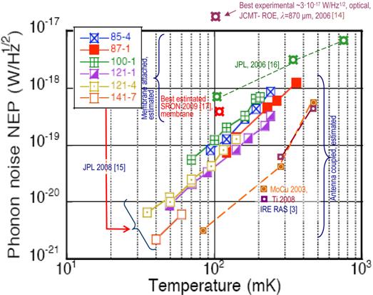
Fig. 8. The NEP’s comparison of nanobolometers, explanation in text.
6. THz radiation image production with sub-diffraction resolution. Described above high sensitive nanobolometer-sensors can be employed in arrays for production of THz radiation image with high definition. Such possibility is very important for THz range where the diffraction diffusion is considerable. One of methods of such procedure is proposed in the laboratory of authors [18]. The method is based on the image scanning using two-dimensional receiving element array when array and image move circularly in common plane relatively each other (rotating or not rotating) with small eccentricity between their centers. The reconstructed image can be obtained by means of the processing the obtained series of scanned images. One of important requirements for obtaining image of high definition is utmost high NEP of nanobolometer-sensor. The results of method application are demonstrated briefly at the Fig. 9. In more details the procedure is described in [18].
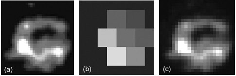
Fig. 9. The illustration of the method: (a) the image obtained at a telescope with high definition and used as comparative one, (b) one of scanned images of the same observed object obtained at a telescope with high diffraction diffusion, (c) the reconstructed image.
7. Conclusion. On the basis of performed consideration the following conclusions are made. (1) Hot-electron nanobolometers with combined radiation absorber and transition edge sensor (TES), the latter fulfill the electron temperature measurement function, are most promising for the achievement of utmost high sensitivity as opposed to bolometers which radiation absorbers made as suspended on membranes and TES’s are membrane temperature sensors. (2) Dimensions of TES have to be small to the limit – thickness down to tens of nanometer, transverse dimensions down to 1 × 0.1 μm2 and operating temperature has to be super low – down to 30 - 40 mK. The networks of immersion lens, planar antenna, microstrip and coplanar lines with nanobolometers coupled into them have to be used to match THz radiation power transfer to so small nanobolometers. Such nanobolometers and arrays of them are needed in the first place for the space astronomical applications where the cosmic background noise is of order of 10-20 W/Hz1/2 and less related to one nanobolometer. The electron-beam lithography technology is needed for fabrication of nanobolometer absorbers-sensors with mentioned above dimensions. The array structures of receiving elements with such nanobolometers are proposed. It is reasonably to be guided to such hot-electron nanobolometers and arrays of them in case of applications demanding the moderate sensitivity (≥ 10-18 W/Hz1/2). In this case they have to have dimensions of order of 10 × 1 μm2 and not too super low temperature (~ 0.3 K).
Acknowledgements. Authors are grateful very much to the International Science and Technology Center for considerable support of the research and development works on grant # 3506.
References.
1. V.V. Schmidt, Introduction to the Physics of Superconductors (in Russian), 2-d ed., Moscow, MCUIE (2000).
2. B.S. Karasik, W.R. McGrath, H.G. LeDuc at al, Supercond. Sci. Technol., 12, pp. 745-747 (1999).
3. A.N. Vystavkin, A.G. Kovalenko, S.V. Shitov at al., J. Comm. Tech. & Electronics, V. 55, 6, pp. 710-715 (2010).
4. A.N. Vystavkin, V.V. Dmitriev, V.V. Zav’yalov at al., ibid, V. 48, 7, pp. 799-801 (2003).
5. G. De Gennes, E. Guyon, Phys. Lett., V. 3, 4,pp. 168-169 (1963).
6. A.N. Vystavkin, A.G. Kovalenko, S.A. Kovtonyuk, J. Comm. Tech. & Electronics, V. 49, 6, pp. 712-715 (2004).
7. B.S. Karasik, S.V. Pereverzev, J. Wei et al., Proc. SPIE, V. 7020, Paper 7020-0E (2008).
8. T. May, G. Zieger, S. Anders et al., Proc. SPIE, V. 6949, Paper 6949-0C (2008).
9. S.V. Shitov , A.N. Vystavkin, Proc. SPIE, V. 7485, Paper 7485-24, pp. 1 - 8 (2009).
10. A.F. Andreev, Sov. Phys. ZhETP, V. 46, 5, pp. 1823-1828 (1964).
11. D. Leisawitz, Ch. Baker, A. Barger et al., Proc. SPIE, V. 6265, Paper 626540 (2006).
12. F. Helmich, R. Ivison, FIRI – a Far-Infrared Interferometer, http://arxiv.org/abs.0707.1822 [PDF only].
13. W. Wild, N.S. Kardashev, Exp Astron, DOI 10.1007/s10686-008-9097-6.
14. James Clerk Maxwell Telescope: http://www.roe.ac.uk/ukatc/projects/scubatwo/
15. B.S. Karasik, S.V. Pereverzev, D. Olaya et al., Proc. SPIE, V. 7020, Paper 7020-13 (2008).
16. M. Kenyon, P. K. Day, C. M. Bradford et al., Proc. SPIE, V. 6275, Paper 627508 (2006).
17. P. Khosropanah, B. Dirks, J. van der Kuur et al., Proc. 20th Int. Symp. on Space THz Tech., April 20-22 (2009).
18. A.N. Vystavkin, A.V. Pestryakov, S.E. Bankov, V.M. Chebotarev, Proc. SPIE, V. 7485, Paper 7485-24 (2009).