|
|
"ЖУРНАЛ РАДИОЭЛЕКТРОНИКИ" "JOURNAL OF RADIOELECTRONICS" N 11, 1999 |
|
RADIATION FROM AN ARRAY OF SLOTTED RADIATORS
Bankov S.E.,
Institute of Radioengineering
and Electronics of RAS
Received November 22, 1999
A diffraction problem for an infinite array of longitudinal slots excited by planar waveguides is considered. An integral equation written relatively electrical field in a slot is obtained and solved with help of Galerkin’s technique for a case of normal radiation from the array. Problems of the array matching in narrow and wide bands are considered.
This work was supported by grant of President of Russian Federation for young doctors of science N99-15-96103.
1. Formulation of the problem
Conventional arrays of printed radiators which are widely used at relatively low frequencies are not optimal for millimeter-wave applications because of high level of dissipative loss in a feeding system, parasitic radiation from its elements, problems with fabrication etc. At the same time low cost and effective antennas for millimeter-wave (MMW) communication systems (Local Multi-Point Distribution Systems (LMDS) for example), traffic control systems and so on are strongly required. An antenna considered in this article looks to be very perspective at MMW because it may be fabricated mostly with help of printed circuits technology and at the same time it does not contain microstrip or analogous printed lines with high loss.
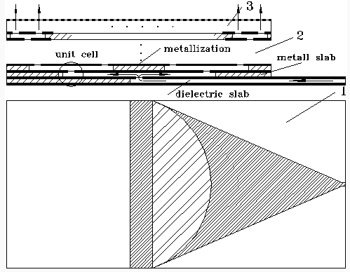
The antenna is shown in fig. 1. It consists of the following three parts: planar waveguide exciter 1, multi-channel divider 2, radiating layer 3. The antenna is supposed to be a narrow beam antenna and therefore its feeding system must produce quasi-uniform two-dimensional phase-amplitude distribution (it is supposed that amplitude distribution may not be perfectly uniform). One-dimensional uniform phase-amplitude distribution may be formed in different ways. In our case this problem is solved by a planar waveguide exciter which as it is shown in fig. 1 may be realized as a planar horn-lens antenna. Printed horn is loaded by a planar lens for phase distribution correction. Such a lens may be also realized as a printed structure. Thus, a guided wave at the horn input (output) is transformed into a plane wave of a planar waveguide (screened dielectric slab). It forms required phase-amplitude distribution only along one axis. Let us note that the exciter 1 being a printed structure at the same time has low dissipative loss because an attenuation constant of a planar waveguide is much smaller then the analogous parameter of a microstrip line.
Fig. 1
Multi-channel divider 2 transforms one-dimensional uniform distribution into two-dimensional one. The divider is a binar-type divider and therefore the number of its output ports is equal to 2N. The main specific feature of the divider is that it occupies several layers connected with each other through the longitudinal slots. Every slot forms a unit cell of the divider. A unit cell of a multi - port divider for antenna applications was previously considered in [1]. Its S-matrix was also obtained in [1]. Thus one can conclude that a problem of the divider analysis is solved because its parameters may be simply calculated now with help of microwave networks theory. Due to this reason a main proplem of the array analysis is a problem of electromagnetic waves radiation from the array. This problem is considered in the article.
The array is supposed to be infinite. One period of the array located at the upper layer ot the discussed antenna (see structure in fig. 1) is shown in fig. 2.
Fig. 2
One can see that the structure is a two - dimensional one. It corresponds to a case of a wide planar waveguide (wide along the OY axis) in which field variations along OY axis are much smaller then along OZ one. However, one should take into account that a solution for case of “narrow” waveguide can be simply obtained from a two-dimensional model by a corresponding replacing of wave numbers [1].
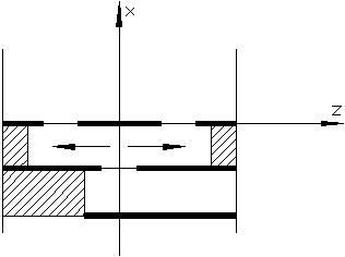
An important property of the array is that its period contains two slots. It is a result of a specific structure of the divider which consists of asymmetrical elementary dividers. However, as it is shown in [1] elementary dividers being asymmetrical in a space have electrical symmetry. Thus, one can suppose that slots are excited by a dominant modes of planar waveguides with the same phases and amplitudes but in every couple of slots this waves propagate in opposite directions.
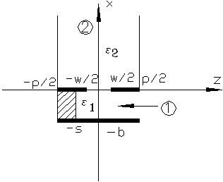
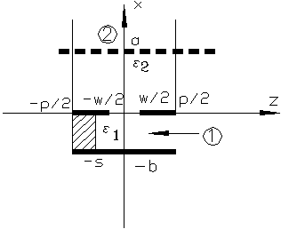
Assumption about electrical symmetry of the elementary divider allows one to conclude that the structure shown in fig. 1 has a plane of symmetry at z=0. Moreover, an electrical wall may be placed at z = 0 without any perturbation of the field. It is well know [2] that electrical walls may be also placed in normally radiated array at z = -p/2 and z = p/2, where p - is a period of an array. Thus, one can see that analysis of the array may be reduced to analysis of a waveguide structure shown in fig. 3.
We have to note that metallizations shown in fig. 3 by thick lines are supposed to be infinitely thin. Then, dielectric constants of regions at x<0 and x>0 are e 1 and e 2 respectively. The structure is excited by an incident TE0-mode of a planar waveguide at x<0. We have to find scattered field and especially amplitudes of reflected wave and waves in waveguide at x>0.
Fig. 3
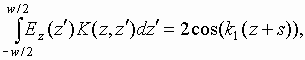
2. Solution of an integral equation
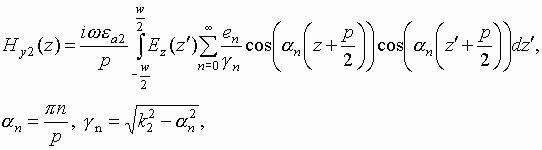
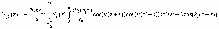
The diffraction problem described above may be reduced to an integral equation written relatively z - component of an electrical field in the slot region. Tangential component of magnetic field Hy may be written at x=+0 (Hy2) and x=-0 (Hy1) in the following way:
|
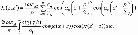
where k1,2 are wave numbers of media’s with dielectric constants e 1 and e 2. Field in the upper region is written in form of infinite sum of normal modes of waveguide at x>0, and field in the bottom region is written in form of Fourier integral. Fields satisfy to all the boundary conditions except condition at x=0, -w/2<z<w/2 where tangential components of magnetic field must be continuos. Field of TE0-mode is written in such a way that it satisfies to boundary condition at z=-s. Because of it the field contains not only incident wave but reflected wave as well. Equalizing Hy1 and Hy2 at x=0, -w/2<z<w/2 one can obtain the following integral equation:
|
|
(1) |
|
|
(2) |
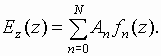
The equation can be effectively solved by Galerkin’s technique. Galerkin’s technique reduces integral equation (2) to a system of linear algebraic equation which can be solved numerically. Unknown function Ez should be written as a sum of basis functions fn with unknown coefficients An:
|
|
(3) |
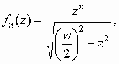
In our case functions fn are taken in the following form:
|
|
(4) |
which satisfies to Meixner’s conditions for field near edges of infinitely thin metallizations [3]. In accordance with Galerkin’s technique the following system of linear algebraic equations may be obtained:
|
|
(5) |
System (5) converges very quickly. Order of the system N may be taken equal to two to obtain S-parameters of the structure with acceptable tolerance.
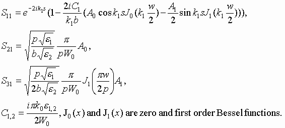
Taking into account that N=2 one can write the following expressions for scattering parameters of the waveguide junction (fig. 3):
|
|
(6) |
Here S11 is a reflection coefficient at port 1 and S21 is a coefficient of transformation of incident wave into a dominant TE0-mode of waveguide at x>0 and S13 is a coefficient of transformation of incident wave into a TE1-mode of waveguide at x>0, W0 is a free space wave impedance. Thus it is supposed that upper waveguide may be a multi-mode one. It means that in a practically interesting range of parameters the array can have two beams. Let us consider this effect in details.
A conventional condition for absence of additional beams in case of infinite normally radiated array has the following form:
|
|
(7) |
where l is a free space wavelength. In our case every propagated mode in the upper waveguide corresponds to a radiating space harmonic in the array. The first higher order mode is non-propagated when:
|
|
(8) |
Thus one can see that condition (8) is much more hard than (7). It is clear now that in a practically interesting range the array can really has two radiating space harmonics. Such an effect is a result of asymmetry of the structure in fig. 3. However, remembering that asymmetry in a space does not always mean electrical asymmetry one can suppose that the considered junction also has electrical symmetry. In this case it means that | S21| >>| S31|. It takes place when Ez in the slot region is close to even function and therefore TE1-mode is not excited at all or is excited with a negligible amplitude. The final answer to this question may be obtained from a numerical solution of the diffraction problem which is discussed in the following chapter.
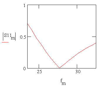
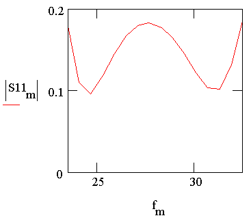
3. Numerical resultsTypical dependence of S11 versus frequency is shown in fig. 4. The plot is calculated for the array with the following parameters: e 1=e 2=1, b=1.7 mm, s=3.2 mm, w=0.95 mm, p=6 mm. One can see that the junction of waveguides is perfectly matched only in one frequency point. Operating frequency range (range in which | S11| is less for example then 0.1) is less then in case of elementary divider [1].
Fig. 4
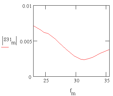
Dependence of S31 modulus versus frequency is shown in fig. 5. One has to take into account that excitation of TE1-mode in the upper waveguide is equivalent to excitation of two space harmonics with propagation constants along
Fig. 5OZ axis equal to - p /p and p /p. Amplitude of space harmonic is equal to one half of amplitude of TE1-mode. Thus, one can see from fig. 5 that in this case array has additional side lobs at the level about - 45 dB. The lobs take a place under the angles about ± 560 relatively OX axis.
We can conclude that the assumed above electrical symmetry of the junction really takes a place in a good approach. However the wider is slot the more intensively TE1-mode is excited and the more asymmetrical is the junction.
As it is following from fig. 4 range of operating frequencies is not wide enough. Let us consider one of the possible ways to make it wider. This way is connected with additional elements inserted to the array. A periodical grating of metal strips may be used as such an element. The array with the additional grating is shown in fig. 6.
Fig. 6
It is well known [4] that the grating with enough small period may be replaced by an infinitely thin film. Fields at the both sides of the film are connected by an impedance type boundary conditions. Impedance of the film has zero real part while its imaginary part is negative. Thus, the grating is a some kind of capacity.
Described above algorithm may be simply generalized to this case. At any rate it takes a place when the distance from array to grating “a” is so long that one can take into account a small number of propagated and non-propagated modes describing interaction between this to objects. Dependence of S11 modulus versus frequency shown in fig. 7 demonstrates possibilities of the grating as a matching element. The plot shown in fig. 7 is obtained for the structure with grating. The rest parameters are the same as in the previous case except b=1.55 mm and s=3.5 mm, a=5.7 mm. Capacity of the grating is equal to 0.0113 pF.
Fig. 7
4. Conclusion
Thus a radiation from an infinite array of specially arranged longitudinal slots is studied. It is shown that the array may be well matched in a wide frequency range. Together with a divider analyzed in [1] this array forms a narrow beam antenna with normal relatively its aperture radiation. The antenna has a multi-layer planar structure that is promising for different applications.
Of course some important problems of antenna design were not considered in this article and in [1]. For example only a division of input power to N equal parts which corresponds to a uniform amplitude distribution at antenna aperture is possible with help of the divider from [1]. However very often it is not an optimal solution and non-uniform distribution may be required. In this case a problem of non-equal power division in elementary divider should be solved. A problem of reducing of number of layers is also actual.
REFERENCES
№ 11, 1999.|
|
|