|
|
"ЖУРНАЛ РАДИОЭЛЕКТРОНИКИ" "JOURNAL OF RADIOELECTRONICS" N 11, 1999 |
|
WAVEGUIDE POWER DIVIDER
,Received November 22, 1999
A divider for planar antennas is considered. The divider is a three-port junction, which divides input power on two equal parts. Junction is formed on the base of planar waveguides. Diffraction problems for junctions of planar waveguides with infinitely thin walls and for walls with finite thickness are considered in the article. S-matrixes for both cases are obtained. Some important for practical design numerical results are presented.
This work was supported by grant of President of
Russian Federation for young doctors of science N99-15-96103.
1. Structure and operating principles of the divider
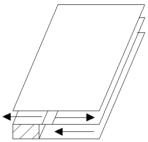
The divider is shown in fig. 1. A planar waveguide is used as a transmition media in this case. It is excited by an incident plane wave which may be produced in different known ways which are not discussed in this article. As it is shown in
fig. 1 planar waveguide in this case is realized as a wide microstrip line which width is much more greater then wavelength. An alternative variant of a planar waveguide is a wide rectangular waveguide. Both structures are very close in electrodynamic content. A solution of electrodynamic problem for a case of planar waveguide without vertical walls may be generalized to a case of rectangular waveguide. It is enough for it to replace wave numbers k1 and k2 to 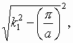 and
and 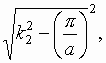 where a is a width of rectangular waveguide (see below about k1 and k2 ). Thus it is reasonable to analyze in details only divider of one type for example a divider on the base of wide microstrip line.
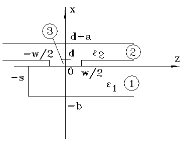
The divider is a planar structure which occupies two layers connected with each other through the longitudinal slots (see fig. 2). One can see that it is some kind of a three-port junction. The central port is located at the lower layer while the rest two ports are located at the upper one. This is a two-dimensional structure (approximately) and one can suppose that the functions describing planar waves amplitude distributions along y-axis at all three ports are identical. Therefore, we may consider this structure as a microwave three-port junction and describe it in terms of S-matrix. In a perfect case element S11 is equal to zero and elements S21 and S31 are equal to each other while its absolute values are equal to 0.707 (equi-phase 3 dB division).
Fig. 1
We have briefly considered operating principles of the proposed divider. A detailed consideration is presented below. Tree-port junction of planar waveguides is considered in the article for two cases: for planar waveguides with infinitely thin walls and for waveguides with walls of a finite thickness. These two cases correspond to two different ways of manufacturing of the divider. A structure with infinitely thin metallization is close to a printed variant of the divider and a structure with a finite thickness of walls is close to a waveguide one. One can say that there is no reasons to consider infinitely thin walls separately. However, a solution obtained for finite thickness metallizations (t¹ 0) can not be used without problems when t=0 or t® 0. Thus, taking into account a practical importance of the last case we will consider it separately.
2. Solution of a diffraction problem for unit cell with infinitely thin metallizations
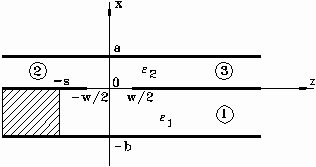
A considered structure is shown in fig. 2. As it was mentioned above it is a three-port junction of planar waveguides. We suppose that dielectric slabs which form this
Fig. 2
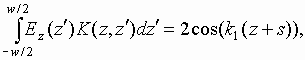
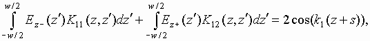
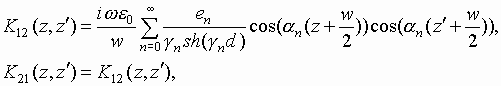
structure have different thicknesses b and a and different dielectric constants e 1 and e 2. The structure is supposed to be two-dimensional (infinite along y-axis). Interlayer metallizations are supposed to be infinitly thin. A diffraction problem is formulated in the following way: a dominant TEM mode of the first planar waveguide (port 1) excites the structure. It is nesessary to find amplitudes of scattered waves at ports 1,2,3. This problem is reduced to a one-dimensional integral equation written relatively unknown electric field component Ez (x=0, -w/2 < z < w/2). The equation has the following form:
where k1=k0![]() , k2=k0
, k2=k0![]() , k0 is a free space wave number,
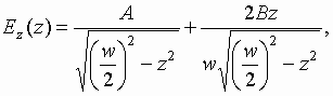
, k0 is a free space wave number, ![]() . Such an equation may be solved by the Galerkin’s technique. Function Ez was approximately written as a sum of two components even and odd:
. Such an equation may be solved by the Galerkin’s technique. Function Ez was approximately written as a sum of two components even and odd:
|
|
(2) |
where A and B are unknown constants. Such a presentation of the function automatically takes into account the Meixner’s conditions for field near a metal edge [2]. In terms of the Galerkin’s method equation (1) is reduced to a system of linear algebraic equations.
Solution of the system allows one to find all the scattering parameters. For example, for S11, S21 and S31 it gives the following expressions:
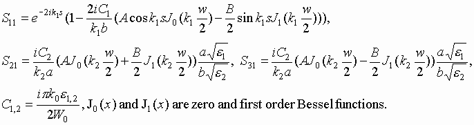
Constants A and B are obtained as a solution of the system of algebraic equations.
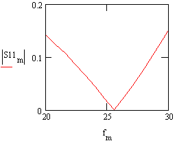
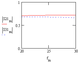
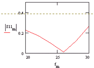
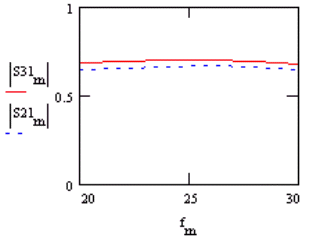
Let us consider now some numerical results. Dependencies of S11, S21, S31 absolute values versus frequency f are shown in fig. 3 and 4.
These plots are obtained for the following parameters: a=1.6 mm, b=1.6 mm, e 1=e 2=2, s=0.2, w=1.6 mm. One can see that the junction is well matched in a wide frequency range. Parameters S21, S31 are not identical due to the structure asymmetry. However difference between them is not sufficient. For example phase difference is not more then 2.3 degree.
An important result is that the junction may contains identical dielectric layers as it is shown above and it does not destroy good matching. This property is very convenient for multi-channel divider design because in this case only substrates of one type are required.
An interesting and important result is that S-matrix elements S21 and S31 are very close to each other (see
fig. 4) that means that the divider divides input power on two equal parts. It is not an evident result because the divider has not geometrical symmetry as a conventional divider. Mentioned electrical symmetry takes a place only in case of small w. The greater is width of the slot the greater is constant B. In all the investigated situations relation ![]() was not more then 0.1. The relation may be used as a measure of electrical asymmetry of the junction. It is important to note that the used approximation of Ez is good for accurate calculations only for relatively small w. In case of wide slots relation
was not more then 0.1. The relation may be used as a measure of electrical asymmetry of the junction. It is important to note that the used approximation of Ez is good for accurate calculations only for relatively small w. In case of wide slots relation ![]() increases and it is nessessary to take into account additional terms. Thus, one can see that the proposed approximation is good in the most interesting range of w values.
increases and it is nessessary to take into account additional terms. Thus, one can see that the proposed approximation is good in the most interesting range of w values.
3. An equivalent circuit of the junction
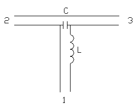
A simple equivalent circuit of the considered above junction may be presented. It is shown in fig. 5.
Fig. 5
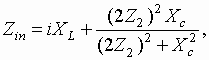
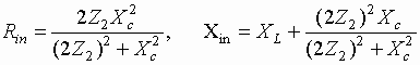
The circuit contains three transmission lines and two reactive elements. Transmission lines correspond to planar waveguides. Two of them have identical characteristic impedances equal to Z2 and the central line has impedance Z1. Transmission lines with impedance Z2 correspond to half infinite planar waveguides at the upper layer and the central line corresponds to planar waveguide at the bottom layer. Shorted waveguide stub at the bottom layer plays a role of an inductivity and slot may be considered as a capacity. Input impedance at port 1 may be expressed in the following way:
|
|
(3) |
where XL and Xc are image impedances of the inductor and capacitor respectively. Real and imaginary parts of the input impedance Zin may be written as
|
|
(4) |
One can see that Xin is equal to zero when:
|
|
(5) |
In case of identical layers Z1 is equal to Z2. In accordance with (4) it can take place when:
![]() .
.
Substituting the last expression to (5) we obtain a solution for XL:
![]()
One can see that the equivalent circuit allows to explain obtained above-mentioned result about perfect matching of a junction with identical layers. The circuit shows that reactive elements play a role of an impedance transformer which transforms input impedance of waveguides at the upper layer (2Z2) to characteristic impedance of a waveguide at the bottom layer Z2. It can not be achieved at very low frequencies when an influence of reactive elements is not sufficient. It is only high frecuency effect.
Simple approximate formulas may be proposed for the equivalent circuit elements:
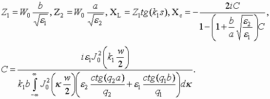
|
(6) |
4. Solution of a diffraction problem for unit cell with finite thickness of metallizations
Unit cell for this case is shown in fig. 6.
Fig. 6
In this case the diffraction problem which is formulated in the same way as it was described above is reduced to a system of integral equations:
|
(7) |
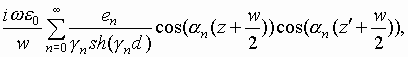

where Ez- is electric field at x=0, -w/2<z<w/2 and Ez+ is electric field at x=d, -w/2<z<w/2.
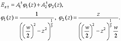
Unknown functions Ez± may be approximated by the following two functions:
|
|
(8) |
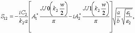
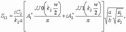
Presented above functions satisfy to Meixner’s conditions for metallization with a finite thickness. The approximation (8) contains odd and even parts and may be used for accurate calculations when w is enough small (see above). Presented system of integral equations with help of approximation (8) is reduced to a system 4x4 of linear algebraic equations written relatively constants ![]() . Solution of the system allows to obtain the following expressions for scattering
parameters:
. Solution of the system allows to obtain the following expressions for scattering
parameters:
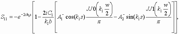
|
(9) |
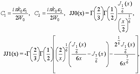
where ![]() - Bessel functions of indexes 1/6 and 7/6.
- Bessel functions of indexes 1/6 and 7/6.
Fig.9
Electrical field distribution in the slot aperture is approximately symmetrical (see fig. 9). Due to this reason S-matrix elements S12 and S13 are close to each other that is equivalent to electrical symmetry of the junction.
5. Computational features
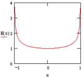
The numerical solution has only one problem - calculation of coefficients of systems of algebraic equations which are obtained in terms of Galerkin’s technique. Typical coefficient may be written as the following integral:
|
|
(10) |
Such an integral can not be directly calculated because the function f(k) slowly decreases as 1/k 2 when k ® ¥ . This problem may be solved in the following way. Let us rewrite the integral (10):
|
|
(11) |
where b is an arbitrary positive constant. One can see that the function j (k ) decreases at infinity as 1/k 4. An additional integral in (11) is a function of one variable
![]()
This function should be calculated one time in a set of points yn. Then calculated values are used to create a spline approximation (it is called as F(y)) of the original function. Function F(y) may be rapidly calculated numerically. Thus we reduce an original slowly converging integral to sum of rapidly converging integral and a simple function.
One can see that function f(k ) has poles in points k = ± k1. This fact also means that numerical calculation of integral I is impossible. Let us transform an original function f(k) to a convenient for numerical solution form. This transformation gives the following expression for integral I:
|
|
(12) |
Now subintegral function y (k ) is a continuous one and decreases at infinity as 1/k 4. An additional integral in (12) may be calculated analytically. Thus finally we numerically integrate continuous function with a good asymptotic at infinity.
6. Conclusion
One can note that considered junctions are not competely printed structures even in case of infinetly thin metallizations. A shorted stub at the bottom layer is the main non-planar element. It can not be fabricated with help of printed circuits technology. Of course it is a disadvantage of the proposed divider. However, we have to note that a shorting wall may be realized not only as a metall wall as it was supposed above. For example, an array of metall cylinders with enough small period can play a role of such a wall [3]. This cylinders may be realized as metallized holes in a substrate. Producing of such a holes is a typical part of printed circuits technology. Thus one can achieve the same electrical properties as has divider considered in the article applying only low cost printed circuits technology. Nevertheless both srtructures are not absolutely identical and a complete study of the last one should be a subject of separate investigation.
REFERENCES
B. Noble. Wiener – Hopf Technidue. Pergamon Press, N.Y. , 1958.
Makoto Ando, Jiro Hirokawa, Tetsuya Yamamoto, Akira Akiyama, Yuichi Kimura and Naohisa Goto. Novel Single-Layer Waveguides for High-Efficiency Millimeter-Wave Arrays // Microwave Theory and Techniques, 1998, vol. 46, N 6 p.p. 792-799.
|
|
|