A Coplanar Waveguide-fed Ultra Wideband Hexagonal Slot Antenna with WLAN Band Rejection
Tapan Mandal 1, Santanu Das 2
1 Department of Information
Technology, Government College of Engineering and
Textile Technology, Serampore, Hooghly, India
2 Department of Electronics & Tele-Comm. Engineering, Bengal Engineering and Science University,
Shibpur, Howrah, India
The paper is received June 15, 2013
Abstract. In this paper a printed regular hexagonal slot antenna with a hexagonal stub fed by a CPW line has been considered for UWB. This antenna is then modified to obtain band rejection for WLAN of 5.15-5.88 GHz by incorporating a C-shape slot within the exciting stub. The parameters of the C-shape slot offer sufficient freedom for selecting and shifting the notch band. VSWR, gain and radiation characteristics of them are studied and discussed here. From the experimental results it has been observed that the impedance bandwidth, defined by VSWR ≤ 2, reaches a value of 7.35GHz (3.05~10.4GHz), with stop band between 5.10 to 6.0 GHz. The antenna gain varies from 4 dB to 6 dB over the whole operating band excluding the notch band. Surface current distributions and transmission line model are used to analyze the effects of the slot. Measured group delay has small variation within the operating band except notch band and hence the proposed antenna may be suitable for UWB applications.
Keywords: CPW, C-slot, hexagonal slot, hexagonal stub, WLAN band, UWB.
1. Introduction
US-Federal Communication Commission (US-FCC) allocated VSWR ≤ 2 bandwidth of 7.5 GHz (3.1–10.6 GHz) for ultra–wideband (UWB) communication [1]. Printed slot antennas are currently under consideration for UWB systems due to their low profile, lightweight, wide bandwidth and omni-directional characteristics. This type of antenna has been realized by using either microstrip line [2-6] or coplanar waveguide (CPW) feeding structure [7-15]. Microstrip fed hexagonal [4], tapered [5] semicircle [6], circle [8] and ellipse [8] shape wide slot antennas are found to have VSWR ≤ 2 bandwidth (BW) for UWB application. A compact hexagonal wide slot antenna with microstrip fed monopole for UWB application has been described [4] but its structure is complex with double metallic layer. The CPW fed hexagonal monopole antennas are found to have 10 dB return loss bandwidth for UWB application [10] with large size structure. In particular, researchers and industry people pay much attention in CPW fed antennas because of their many attractive features such as, simple structure of a single metallic layer, low radiation loss and easy integration with integrated circuits [7-9]. The UWB antenna has numerous applications such as remote sensing, radar, imaging, localization and medical applications.
In this paper a printed hexagonal slot (aperture) antenna with a hexagonal stub is proposed for UWB applications. The patch (stub) is fed by a CPW line such that single-layer metallization substrate is required for this antenna.
However, the existing Wireless Local Area Network (WLAN: IEEE 802.11a) service bands (5.15 - 5.88 GHz) are responsible for the performance degradation of UWB system because of the interference. To overcome this problem, an UWB with band rejection characteristic is desirable. In the conventional design, band stop filter are added at the end of the antenna or the devices. Thereby the size of the antenna is increased. Several UWB antennas with band rejection characteristic have been proposed [3,5,10,13-15]. For printed monopole antennas, the most familiar methods to achieve band-notched function are etching slots on the metallic patch, feeder or the ground plane [9-11] in different shapes such as C-shaped [13], U-shaped [4,6], L-shaped [10] slot etc. The band notch performance is achieved by placing parasitic strips in close proximity to the antenna [10]. In this paper, the filter response is achieved by etching a thin C- slot on the exciting stub. The slot creates a narrow frequency rejection without disturbing the rest of the operating frequencies and radiation performances. Tuning effects of major parameters on the stop band performance are simulated and analyzed also. Compared to the circular, elliptical, hexagonal, tapered slot [4,5, 12,13], the proposed hexagonal-shaped slot with hexagonal stub has three advantages. These are:
1. The antenna can be simply extended to the advanced band notched design without changing the dimensions of the exciting stub as well as aperture of the prototype antenna.
2. The exciting stub has a simple geometry with less number of design parameters.
3. The computation time is less for optimization of process.
All of the simulations are carried out using a Method of Moment (MoM) based IE3DTM simulation software [15]. VSWR, input impedance, gain, radiation patterns, group delay and phase characteristics are studied and analyzed.
2. Antenna Design Considerations
For UWB antennas lower band edge frequency and entire band width become the design parameters instead of resonant or operating frequency [2]. The prototype antenna is designed on a substrate having dielectric constant (εr) = 4.4 and thickness (h) = 1.59 mm (Fig. 1). The lower frequency (fl) has been determined using a formula [13,14] given in equation (1)
 (1)
(1)
where![]() is the effective relative permittivity. c and Rs
are velocity of light and aperture (slot) radius respectively.
is the effective relative permittivity. c and Rs
are velocity of light and aperture (slot) radius respectively.
Here side length of the aperture (Lp) is related to the aperture radius (Rs) and height of the slot (H) is related to the side length as given follows
![]()
![]() (2)
(2)
![]() (3)
(3)
where Lp and H are the side length and height of hexagonal slot.
The hexagonal exciting stub dimension is then considered with respect to the aperture radius as
![]() (4)
(4)
The radiating element, namely the aperture, is chosen hexagonal in the investigation order to achieve a wide BW. A 50Ω CPW transmission line is designed having a strip width of 3.8 mm. The gap between the feed line and the coplanar ground plane is 0.4 mm. The detailed dimensions are shown in Table 1.
In another form (Fig. 2) the hexagonal slot antenna is made on the same substrate with the dimensions same as before. In order to reject WLAN band frequencies a thin C-slot is made on the exciting stub. Usually, the length of the slot is made approximately equal to half of the guided wavelength at the notch frequency of the band. This is given by
 (5)
(5)
![]() (6)
(6)
where Ltotal is the length of the slot. Corresponding to f notch= 5.47 GHz the lengths of the slots can be calculated as 17.4 mm. The optimum slot width is found to be 0.3 mm by way of simulation.
|
Fig.1. Prototype of Regular Hexagonal slot antenna |
Fig.2. Hexagonal slot antenna with c-slot (proposed) |
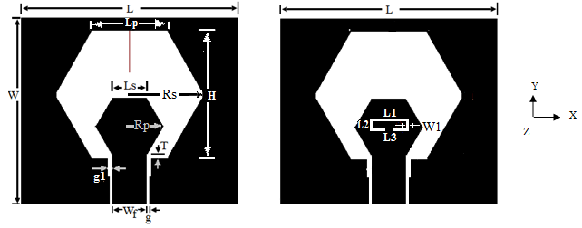
Table 1: Optimized parameter for the proposed antenna
|
Parameter |
L |
W |
Rs=Lp |
Ls =Rp |
H |
T |
Wf |
g |
g1 |
L1 |
L2 |
L3 |
W1 |
|
Dimension (mm) |
42 |
38 |
13.5 |
6.5 |
22.5 |
0.3 |
6.5 |
0.4 |
0.7 |
7.15 |
2 |
0.5 |
0.3 |
3. Parametric Study and Discussion
For the layout of the prototype antenna given in Fig.1 the effects of extrusion depth T on the input impedance are simulated and shown in Fig. 3. It is observed that the T mainly influences the impedance on middle frequencies (4–5 GHz). The hexagonal aperture (Rs) is important for the lower frequency. As the slot radius value (Rs) increases, the lower frequency is shifted to the left side of the VSWR plot (Fig.4). Thus aperture radius plays a significant role for selecting the lower edge of the band. Fig. 5 indicates that the hexagonal stub (Rp) mainly influences the impedance at lower frequencies (3.8 – 4.5 GHz).The step type ground plane near the feed is considered for impedance matching resulting in wide BW (Fig. 6). From the surface current distribution, it has been observed that the hexagonal slot produces resonance at lower frequency. The hexagonal stub yields second resonance and steps in the ground plane is responsible for the third one.
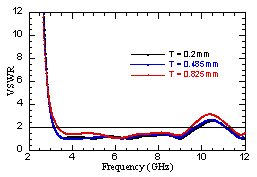
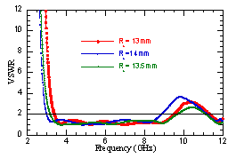
Fig. 3 Simulated VSWR for several of T Fig. 4 Simulated VSWR for different Rs
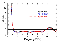
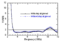
Fig. 5 Simulated VSWR for different Rp
Fig. 6 Simulated VSWR with step and without
step at ground plane
Next the parametric study and analysis are carried out for the antenna with WLAN band rejection (Fig. 2). The simulated VSWR characteristics for various values of Ltotal and W1 are shown in Fig. 7 and Fig. 8 respectively. As the total slot length rises, the stop band region moves toward the lower frequency with higher VSWR peak. Slot length has greater impact than slot width on shifting the frequency as is evident from Fig. 7 and Fig. 8. Fig. 9 indicates the VSWR versus frequency characteristics of the proposed antenna for various values of loss tangent. From the characteristics, it is observed that the peak value of VSWR at notch frequency decreases while the loss tangent of the substrate increases. Due to the presence of C-slot inside the patch, maximum current flows back to the feeding part and degenerates radiation around 5.10 GHz to 5.88 GHz.
The simulation responses of prototype antenna exhibit 6.5GHz (3.10 ~ 9.6 GHz) 2:1 VSWR impedance BW shown in Fig. 4 for T = 0.485 mm, Rp = 6.5 mm and Rs = 13.5 mm. The simulated VSWR characteristics in Fig. 7 of proposed antenna reveals stop bands of 0.78 GHz (5.1-5.88 GHz) for VSWR ≤ 2 within the frequency span from 3.1 GHz to 9.6 GHz.
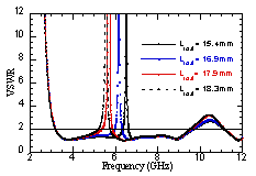
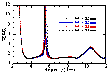
Fig. 7 Simulated VSWR for various lengths of Ltotal Fig. 8 Simulated VSWR for various width
of W1
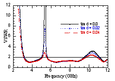
Fig. 9 Simulated VSWR for different values of loss tangent.
4. Fabrication and Measurements
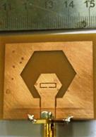
Photograph of the prototype and proposed antenna are shown in Fig. 10. The following antennas are fabricated on the same specification substrate as mentioned in section 2. An Agilent make (Model: N5230A) vector network analyzer is used for VSWR measurement. The simulated and measured VSWR performances of prototype antenna (Fig. 10(a)) are plotted in Fig. 11 for comparisons. The experimental response yield 6.8 GHz (3.2 GHz – 10.0 GHz) 2:1VSWR impedance band. A good agreement between simulation and measurement is achieved. The simulated and measured VSWR responses of proposed antenna (Fig. 10(b)) are shown in Fig. 12. The simulated VSWR characteristic reveals stop band of 0.78 GHz (5.10-5.88 GHz) for VSWR ≤ 2 within the frequency span from 3.1GHz to 9.6 GHz. The measured characteristic shows 0.90 GHz (5.10 - 6.0 GHz) stop band which cover the entire WLAN band in frequency span of 3.05 – 10.4 GHz. The dimensional mismatch between simulated and physical structures and wide flange of the SMA connector used for measurement may cause the discrepancy between the simulated and measured results in higher frequency band. The loss tangent of the substrate may cause the difference between simulated and measured results at the notch frequency (5.5 GHz).

(a) (b)
Fig. 10 Fabricated structure of (a) prototype (b) proposed
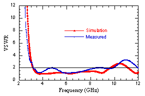
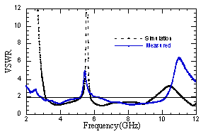
Fig. 11 Measured and simulated VSWR of Fig. 12 Measured and simulated VSWR of
the prototype antenna the proposed antenna
5. Radiation Pattern
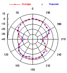
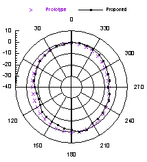
(i) at 3.47 GHz (a) E-plane pattern (b) H-plane Pattern
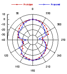
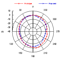
(ii) 8.3 GHz (a) E-plane pattern (b) H-plane Pattern
Fig. 13 Measured radiation pattern characteristics for prototype (Fig. 10(a)) and proposed antenna (Fig. 10(b))
The measured co-polar radiation patterns at 3.47 GHz and 8.3 GHz are shown in Fig. 13. At lower frequencies H-plane radiation patterns are omnidirectional, whereas in E-plane, it is figure of eight because of small ground plane on the same side of stub At higher frequencies, radiation patterns are changing with small variation. The main reason of change is the higher mode excitation by the structure. It is noted that adding a slot in the patch does not significantly alter the radiation patterns of the antenna. The patterns are reasonably stable in entire UWB region and so can be considered as a good UWB antenna.
6. Input Impedance and Gain
The real and imaginary part of the simulated input impedance versus frequency of proposed antenna is shown in Fig. 14. The real part of the antenna impedance varies around 50Ω, while its imaginary part has small values and oscillates around zero. This is mainly because a continuous coupling is obtained between hexagonal patch and ground plane at different positions, and hence matching is achieved for different frequencies. The step in the ground plane creates a capacitive load that neutralizes the inductive nature of the patch antenna to produce nearly-pure resistive input impedance. The impedance of the structure changes acutely making large reflection which results in steep rise of VSWR and also sharp decrease of gain as shown in Fig. 15. The proposed antenna simulated gain varies from 4 – 6 dB over the 3.10 – 9.6 GHz range except in notch band.
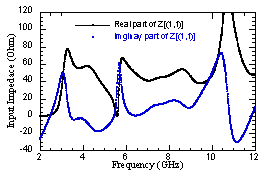
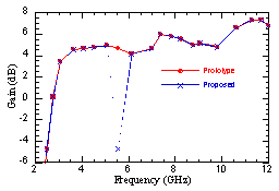
Fig. 14. Simulated input impedance of proposed antenna Fig. 15 Simulated gain versus frequency plot
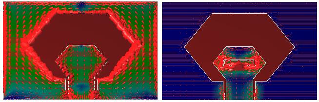
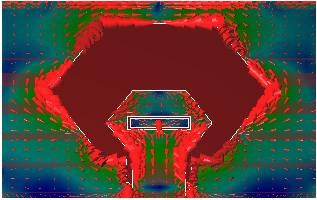
7. Current Distribution and Analysis
Surface current distributions of the antenna with C-slot at different frequencies are shown in Fig. 16. At a pass band frequency, surface current are passing through the patch but at notch band frequency, most of the surface currents are concentrated around the slot. Therefore slot stops the surface current and as a result notch band is obtained. Therefore transmission is negligible at the notch band. At a pass band frequency of 3.47 GHz and 8.86 GHz (outside the notch band) the distribution of surface current is uniform as shown in Fig. 16(a) and Fig. 16(c) respectively. In Fig. 16(b) at the notch frequencies, the current distribution is concentrated and oppositely directed on the interior and exterior side of the slot. This causes the antenna to operate in a transmission-line-like mode, which transforms the nearly zero impedance (short circuit) at the top of the slot to nearly infinite impedance (open circuit) at the antenna feeding point [17]. This infinite impedance at the feeding point leads to the desired impedance mismatching model which is depicted in Fig. 17(b). At the notch band, when the L total = λ/2, stub1 works as a quarter-wavelength transmission line terminated in a short circuit. Therefore stub1 behaves as an open- circuited series stub with infinite input impedance (Z in = ∞) [18], causing a total impedance mismatch between the feed line and the radiating patch and so the notch band is generated. The conceptual circuit model for proposed antenna, which has a series stub with antenna resistance (Ra) as illustrated in Fig 17(a).
(a) 3.47GHz (b) 5.5GHz
![]() Min
Min
(c) 8.86GHz
Fig. 16 Surface current distributions of proposed antenna; (a) pass band (b) stop band and (c) pass band
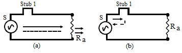
Fig. 17 Transmission line model for the antenna at (a) pass band (b) notch band
8. Transfer Function and Time Domain Study
Agilent make Vector Network Analyzer is used for the time domain characteristics study. The group delay, magnitude and phase of S21 are measured between the two identical antennas which are oriented in face to face mode with a distance of 150 mm. Fig.18 shows the measured magnitude of S21 and group delay for the antenna system. From Fig. 18, it is observed that the magnitude of S21 is relatively flat (variation less than 10 dB) from 3 GHz to 9 GHz. The variation of group delay for proposed antenna is within 1 ns across the frequency range from 3.05-10.4 GHz except notch band, in which the maximum group delay is more than 10 ns in 5.5 GHz notch. The measured group delay corresponds well to the phase of S21 (Fig. 19), so it proves that the antenna has a good time-domain characteristic and a small pulse distortion as well. Therefore it may be considered as a UWB antenna.
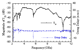

Fig. 18 The measured magnitude of S21 and group delay of Fig.19 The measured phase of S21 for the proposed
the proposed antenna systems antenna systems
9. Conclusions
To mitigate the interferences between the UWB systems and existing WLAN system, a CPW fed aperture antenna with band rejection has been proposed. One half wave length C-slot is added in the hexagonal stub for rejection of WLAN band in UWB region. The surface current distribution and transmission line model are used to analyze the physical effect of the slot generating the band notched characteristics. This antenna has ultra wide-band performance in the frequency band of 7.35 GHz (3.05 to 10.4 GHz) for VSWR ≤ 2 with excellent WLAN rejection band. The radiation patterns are stable over UWB region except stop band. The antenna has appreciable gain in the UWB band. It has been revealed that the antenna has linear phase of transfer function and constant group delay within the operating band except at notch band which ensures the good linear transmission performances. Therefore the proposed antenna is expected to be a good candidate in various UWB applications.
Acknowledgement
This work was supported by CSIR, New Delhi, India. Sanctioned No: 22(0512)/EMR-II dt. 31.05. 2010.
References
[1] First Report and Order, “Revision of Part 15 of the commission’s Rule Regarding Ultra-wideband Transmission system FCC 02-48”, Federal Communications Commission, 2002.
[2] H. L. Lee, H. J. Lee, J. G. Yook, and H. K. Park, “Broadband planar antenna having round corner rectangular wide slot”, in Proc. IEEE Antennas and Propagation Society Int. Symp.,vol. 2, pp. 460–463,2002.
[3] F. Li, L.S. Ren, G. Zhao and Y.C. Jiao, “A compact microstrip line fed slot antenna with dual band notched characteristics for WLAN / WiMAX applications”, Progress In Electromagnetics Research Letters, vol. 16, pp.89-97, 2010.
[4] Mohammad Reza Ghaderi and Farzad Mohajeri,“A compact hexagonal wide slot with microstrip fed monopole for UWB application”, IEEE Antennas and Propagation Letter, vol. 10, pp. 682-685, 2011.
[5] Rezaul Azim, Mohammad Tariqul Islam and Norbahiah Misran, “Compact tapered shape slot antenna for UWB applications”, IEEE Antenna and Propagation Letter, vol. 10, pp. 1190-1193, 2011
[6] X. J. Liao, H. C. Yang, N. Han and Y. Li, “Aperture UWB antenna with triple band-notched Characteristics”, Electronics Letters, vol. 47, no. 2, 2011
[7] J. Y. Chiou, J. Y.Sze, and K. L.Wong, “A broad- band CPW-fed strip loaded square slot antenna”, IEEE Trans.Antennas Propag., vol. 51,no. 4, pp. 719–721, 2003.
[8] Xian Ling Liang, Tayeb A. Denidni, Li Na Zhang, Rong Hong Jin, Jun Ping Geng and Quan Yu,“Printed binomial curved slot antennas for various wideband applications,” IEEE Transactions on Microwave Theory and Techniques, vol. 59, no. 4, pp.1058-1065, 2011.
[9] H. Chen, Y. Ding, and D. S. Cai, “A CPW fed UWB antenna with WiMAX/WLAN band notched characteristics”, Progress In Electromagnetics Research Letters, vol. 25, pp.163-173, 2011.
[10] Yi-Cheng Lin, and Kuan-Jung Hung, “Compact Ultra wideband and Rectangular Aperture Antenna and Band-Notched Designs”, IEEE Transactions on Antennas and Propagation, vol. 54, no.11, pp. 3075-3081, November 2006.
[11] K. P. Roy and S. Tiwari, “Ultra wide band hexagonal monopole antennas,” IET Microwaves, Antenna and Propagation, vol. 4, Iss. 4, pp.437-445, 2010.
[12] Pengcheng Li, Jianxin Liang and Xiaodong Chen, “Study of printed elliptical/circular slot antennas for ultra-wide band applications”, IEEE Transactions on Antennas and Propagation, vol. 54, no. 6, pp. 1670- 1675, 2006.
[13] M.A. Habib, A. Bostani Djaiz, M. Nedil, M.C.E.Yagoub and T. A. Denidni,“Ultra Wideband CPW – fed aperture antenna with WLAN Band Rejection”, Progress In Electromagnetics Research, vol.106, pp.17-31, 2010.
[14] M. Abdollahvand, G. Dadashzadeh, and D. Mostafa,“Compact Dual Band-Notched Printed Monopole Antenna for UWB Application”, IEEE Antennas and Wireless Propagation Letters, vol. 9, pp. 1148-115, 2010.
[15] A.F.Sun,Y.Z.Yin,S.H.Jing,Y.Yang,B.W.Liu and Z.Li, “Broadband CPW-Fed Antenna With Band-Rejected characteristics for WLAN/WiMAX Operation,” Progress In Electromagnetics Research C, Vol. 22,pp.47-54, 2011.
[17] D. M. Pozar, “Transmission line theory,” in Microwave Engineering, 3rd ed. New York: Wiley, 2005, pp. 49–90.
[18] Trang Dang Nguyen, Dong Hyun Lee, and Hyun Chang Park, “Design and Analysis of Compact Printed Triple Band-Notched UWB Antenna”, IEEE Antennas and Wireless Propagation Letters, vol. 10, pp.403-406, 2011.