Modeling and Validation of Loose Coupler by Using DGS in Branch line Coupler
1Tamasi Moyra, 2Susanta Kumar Parui, 2Santanu Das
1Department of Electronics and Communication Engineering,
National Institute of Technology, Agartala
2Department of Electronics and Telecommunication Engineering,
Bengal Engineering and Science University, Shibpur, www.becs.ac.in, India
Received November 9, 2012
Abstract. A novel planar 10 dB loose branch line coupler is proposed for application to the 2.5 GHz centre frequency. This proposed coupler is implemented with rectangular ring headed dumbbell shaped Defect Ground Structure (DGS) along with conventional microstrip transmission line. Design of this conventional branch line coupler with DGS provides more design flexibility. Use of DGS underneath the microstrip line increases the electrical length of microstrip line, provides slow wave characteristics and increases the impedance of the microstrip line. In this paper one high impedance microstrip line is easily implemented by using proposed DGS structure which is required for designing the loose coupler. Finally, the compact branch line 10 dB loose coupler is designed, fabricated and measured. The experimental results are in good agreement with predicted simulated values.
Keywords: branch line coupler, Defect Ground Structure (DGS), 10 dB loose coupling, microstrip line.
I. INTRODUCTION
The branch-line coupler [1] plays an important role in microwave and millimeter wave circuits. There are lots of applications of hybrid branch-line 3-dB or 6-dB tight couplers in our modern microwave and millimeter wave communication systems. Those tight couplers can be easily designed using transmission line in a conventional way. But design of loose coupler is quite different.
A transmission line with etched defects on metallic ground plane such as two-dimensional photonic Band Gap (PBG) and one-dimensional Defected Ground Structure (DGS) has been studied in microwave and millimeter-wave frequency ranges [1-3]. Applications of a microstrip line with DGS structure include slow-wave structure, harmonic rejections with compact dimensions and low-loss characteristic, various circuit design, and so on [4]-[6]. Etched defects on metallic ground plane of a microstrip line provide higher effective permittivity and characteristic impedance than those of the conventional microstrip line due to increase of the electric length and effective inductance of transmission lines [4-9]. Microstrip line with DGS increases the group velocity delay due to the steep phase characteristic. Delay of the group velocity reduces the dimension of distributed components in RF and microwave integrated circuits.
In this paper, one branch-line coupler with rectangular ring headed dumbbell shape DGS is proposed in order to implement loose coupling characteristics of 10 dB, which requires for the realization of high impedance line. Requirement of the high impedance line section faces with restrictions such as impractical very narrow transmission line width in implementation of designed circuits. In this paper, the DGS structures are used to implement the high impedance line section. Use of the DGS section makes it easy to control the characteristic impedance of microstrip line and provides design flexibility. Since DGS section can increase the electrical length and effective inductance of microstrip line hence the conductor width with DGS section for a determined characteristic impedance is wider than that of conventional microstrip line. The coupling can be controlled by changing the physical dimensions of the DGS and adjusting the length and width of the microstrip line. Finally, a 10-dB loose branch-line coupler operating at 2.5 GHz is optimally designed, fabricated and measured.
II. GENERAL STUDY AND CALCULATION OF IMPEDANCES
(a) General Study of Branch-line Coupler:
Fig. 1 shows a branch-line coupler. It consists of two quarter-wave-long
(![]() ) transmission line sections of
characteristic impedance
) transmission line sections of
characteristic impedance![]() each,
connected by two shunt branches. The shunt branches are quarter-wave-long (
each,
connected by two shunt branches. The shunt branches are quarter-wave-long (![]() ) transmission line sections of
characteristic impedance
) transmission line sections of
characteristic impedance![]() each. By
selecting the appropriate values of
each. By
selecting the appropriate values of ![]() and
and![]() , the circuit can be made to operate like
a directional coupler.
, the circuit can be made to operate like
a directional coupler.
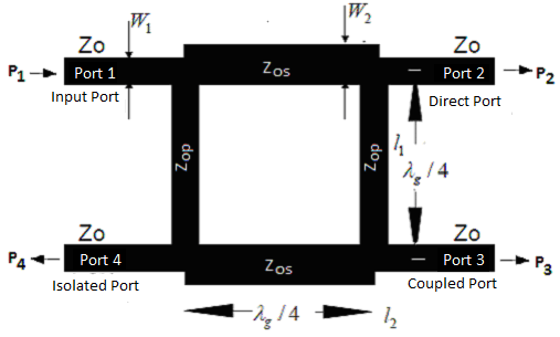
Fig. 1. Layout of a branch-line coupler in planar circuit configuration
At the center frequency the scattering parameters of a branch-line coupler are given by


Where, ![]() denotes the impedance of various ports of
a branch-line coupler. The scattering parameters of a branch-line coupler also
satisfy the following condition, which follows from the principle of
conservation of energy:
denotes the impedance of various ports of
a branch-line coupler. The scattering parameters of a branch-line coupler also
satisfy the following condition, which follows from the principle of
conservation of energy:
![]()
Where, it is
assumed that S11=S41=1. Substituting the values of
scattering parameters from equations (1) and (2) it is found that ![]() and
and![]() should
satisfy the following condition:
should
satisfy the following condition:

A branch-line coupler as shown in Fig.1 has two planes of symmetry. The scattering matrix of a branch line coupler can therefore be expressed as,
![]()

The characteristic impedances of the main-line and shunt branches of a branch-line can be computed using equations (1) and (2) as
![]()
and

Zos and
Zop are the required main line and shunt branch line
characteristic impedances of any branch-line coupler.
(b) Calculation of Zos and Zop for 10-dB coupler:
Consider all ports are
matched to 50![]() microstrip transmission line
i.e.
microstrip transmission line
i.e. ![]() . For 10 dB branch line coupler
coupling from port 1(Input port) to port 3 (coupled port ) is 10 dB.
. For 10 dB branch line coupler
coupling from port 1(Input port) to port 3 (coupled port ) is 10 dB.
i.e. ![]()
or,
![]()
or,
![]() ……………………………………(10
a)
……………………………………(10
a)
Now, from equation (5) , it can be obtained
![]() ………….......…………………..(10
b)
………….......…………………..(10
b)
Using equation (8) and (9), we have,
![]() ………………...……………...…….(11 a)
………………...……………...…….(11 a)
and
 ……………….…………………………..(11
b)
III. EFFECT OF DGS ON CHARACTERISTIC IMPEDANCE
One microstrip transmission line of length 16.4mm and width 3mm with FR4
substrate (of dielectric constant 4.4 and substrate height 1.59mm with
negligible loss tangent) provides 50![]() characteristic
impedance at 2.5 GHz. This characteristic impedance can be controlled by
introducing DGS underneath a microstrip line. For simplicity, let there is a
rectangular ring headed dumbbell shaped DGS underneath a 50
characteristic
impedance at 2.5 GHz. This characteristic impedance can be controlled by
introducing DGS underneath a microstrip line. For simplicity, let there is a
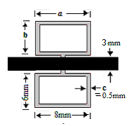
rectangular ring headed dumbbell shaped DGS underneath a 50![]() microstrip line as shown in Fig. 2(a) and
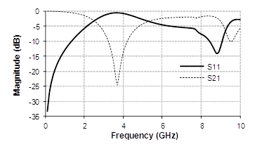
the simulated magnitude responses or scattering parameters are shown in Fig. 2(b).
Simulation has been done with IE3D electromagnetic simulator. As an example one
rectangular ring dumbbell DGS of head length, a = 8mm and breadth, b = 6
mm and width, c = 0.5mm and two heads are connected with transverse slot of
length 4mm and width 0.5mm is etched in the ground plane of the microstrip
line. One remarkable advantage of using the DGS under the microstrip line is
that it can increase the characteristic impedance by the additional effective
inductance generated by the loop of DGS structure. The addition of this
extra inductance causes the characteristic impedance of the microstrip line to
be much higher than that of a conventional microstrip line with the same
conductor width.
microstrip line as shown in Fig. 2(a) and
the simulated magnitude responses or scattering parameters are shown in Fig. 2(b).
Simulation has been done with IE3D electromagnetic simulator. As an example one
rectangular ring dumbbell DGS of head length, a = 8mm and breadth, b = 6
mm and width, c = 0.5mm and two heads are connected with transverse slot of
length 4mm and width 0.5mm is etched in the ground plane of the microstrip
line. One remarkable advantage of using the DGS under the microstrip line is
that it can increase the characteristic impedance by the additional effective
inductance generated by the loop of DGS structure. The addition of this
extra inductance causes the characteristic impedance of the microstrip line to
be much higher than that of a conventional microstrip line with the same
conductor width.
|
Fig. 2(a). Rectangular ring dumbbell DGS |
Fig.
2(b). Scattering parameters |
The equivalent circuit of the microstrip line with DGS is shown in Fig.3. Then, the equivalent characteristic impedance and electrical length of the microstrip line with DGS are determined [9] from the S-parameters calculated by simulation.
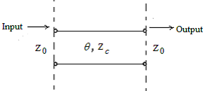
Fig.3. Equivalent circuit of the DGS section, and Z 0 is the reference impedance.
The S 21 can be expressed as following:
 ………………………………………..………(12)
The variable m is:
 ………………………………………..……….…….(13)
The constant θ
is the electrical length. Then, m and θ can be derived from the
magnitude ![]() and phase (φ 21)
of S21 :
and phase (φ 21)
of S21 :
 ……………………………..…………...…..(14)
 …....……………… ….…..(15)
Then, the equivalent characteristic impedance is:
 …………………………… .…..(16)
When the electrical length θ is quarter wavelength, the equivalent characteristic impedance of the microstrip line with DGS is calculated as following:
 ………………………………………....…..……(17)
![]() …………………………………………………..….(18)
…………………………………………………..….(18)
The variable Z in is the input impedance toward the DGS section and Γ denotes the input reflect coefficient.
From the above concept and equations it is possible to find the effective
characteristic impedance of the microstrip line with DGS. Now, in the taken
example in Fig. 2(a) the 3mm width microstrip line provides 50![]() characteristic impedance without DGS at
operating frequency 2.5 GHz. i.e. Z0 = 50
characteristic impedance without DGS at
operating frequency 2.5 GHz. i.e. Z0 = 50![]() . But introducing DGS provides the
scattering response as Fig. 2(b), from Fig. 2(b) and equation (17) and (18) it
can be obtained the effective characteristic impedance of the microstrip line
with DGS is, Zc = 69.775
. But introducing DGS provides the
scattering response as Fig. 2(b), from Fig. 2(b) and equation (17) and (18) it
can be obtained the effective characteristic impedance of the microstrip line
with DGS is, Zc = 69.775![]() .
.
The effective characteristic impedance can be tuned by varying the dimension of one parameter keeping other constant. The following Table 1 shows the different values of effective impedance, Zc with different values of defected head length, a.
Table 1: Variation of Zc with
head length a (with line impedance 50 ![]() )
)
|
Length, a (mm) |
4 |
6 |
8 |
10 |
|
Line imp, Zc ( |
58.8004 |
62.3951 |
69.775 |
88.298 |
IV. DESIGN PROCEDURE OF 10 dB COUPLER
From
the above analysis in section II, it has been observed that there is the
requirement of Z0s = 47.434![]() characteristic
impedance transmission line for the main branch and Z0p = 150
characteristic
impedance transmission line for the main branch and Z0p = 150![]() characteristic impedance transmission
line for shunt branch line. The 10-dB branch line loose coupler has been
designed and fabricated on FR4 substrate of dielectric constant 4.4 and
substrate height 1.59mm with negligible loss tangent. The low characteristic
impedance 47.434
characteristic impedance transmission
line for shunt branch line. The 10-dB branch line loose coupler has been
designed and fabricated on FR4 substrate of dielectric constant 4.4 and
substrate height 1.59mm with negligible loss tangent. The low characteristic
impedance 47.434![]() value of the main line
can be easily implemented with the help of conventional microstrip line of
length 16.4mm with 3.29 mm width at 2.5 GHz. But there is requirement of almost
17mm length and 0.17 mm width microstrip line for the design of150
value of the main line
can be easily implemented with the help of conventional microstrip line of
length 16.4mm with 3.29 mm width at 2.5 GHz. But there is requirement of almost
17mm length and 0.17 mm width microstrip line for the design of150![]() characteristic impedance for shunt branch
line. The fabrication of this too narrow microstrip line is tough enough and
almost impossible. Therefore, an arbitrary rectangular ring headed dumbbell DGS
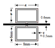
has been introduced underneath a practical width of 0.6mm microstrip line for
designing high impedance shunt branch line as shown in the Fig. 4(a) and the
scattering parameters are shown in Fig. 4(b).
characteristic impedance for shunt branch
line. The fabrication of this too narrow microstrip line is tough enough and
almost impossible. Therefore, an arbitrary rectangular ring headed dumbbell DGS
has been introduced underneath a practical width of 0.6mm microstrip line for
designing high impedance shunt branch line as shown in the Fig. 4(a) and the
scattering parameters are shown in Fig. 4(b).
|
(a) |
(b) |
Fig. 4. (a) proposed DGS, (b) Scattering response
From the above concept obtained from the section III, the effective
characteristic impedance of microstrip line obtained from the above DGS
structure is 165.451![]() . Now, the effective
characteristic impedance of microstrip line can be tuned by changing the
dimension of any parameter of DGS keeping others constant. Considering, width
(b) of the ring head is variable keeping other parameters constant. Then
variation of the reflection coefficient and the characteristic impedance is
shown in Table 2.
. Now, the effective
characteristic impedance of microstrip line can be tuned by changing the
dimension of any parameter of DGS keeping others constant. Considering, width
(b) of the ring head is variable keeping other parameters constant. Then
variation of the reflection coefficient and the characteristic impedance is
shown in Table 2.
Table 2 Variation of ![]() and Zc with ‘b’: with
line impedance 119.47
and Zc with ‘b’: with
line impedance 119.47![]()
|
Ring width, b (mm) |
Reflection coefficient |
Char. Impedance, Zc
( |
|
7 |
1.467 |
177.686 |
|
6 |
1.567 |
164.451 |
|
4 |
1.833 |
142.533 |
Fig. 5 shows the variation of the characteristic impedance Zc with ring width, b as follows:
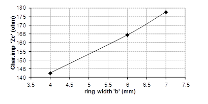
Fig. 5. Ring breath, ‘b’ Vs. characteristic impedance ‘Zc’
From the above Fig. 5 it
is observed that there is the requirement of ring width, b =4.65mm to obtain
the 150 ![]() characteristic impedance. Therefore,
the proposed structure of 10 dB branch line coupler is shown in Fig. 6(a) as
follows:
characteristic impedance. Therefore,
the proposed structure of 10 dB branch line coupler is shown in Fig. 6(a) as
follows:

Fig. 6(a). Proposed 10 dB branch line coupler
The required dimensions of the proposed rectangular ring headed dumbbell
DGS structure for high impedance, 150![]() shunt branch
line are a =8mm, b = 4.65mm, c = 0.5mm and the two heads are separated
by 2mm long, 0.5mm width transverse slot. The others dimensions are L1
= 16.4mm, W1 =3.29mm,W2 = 3mm, L2 = 17mm and W3
= 0.6mm. The above designed structure of 10 dB loose coupler is fabricated on
FR4 substrate and simulated by MoM based IE3D electromagnetic simulator and the
scattering responses are shown in Fig. 6(b).
shunt branch
line are a =8mm, b = 4.65mm, c = 0.5mm and the two heads are separated
by 2mm long, 0.5mm width transverse slot. The others dimensions are L1
= 16.4mm, W1 =3.29mm,W2 = 3mm, L2 = 17mm and W3
= 0.6mm. The above designed structure of 10 dB loose coupler is fabricated on
FR4 substrate and simulated by MoM based IE3D electromagnetic simulator and the
scattering responses are shown in Fig. 6(b).
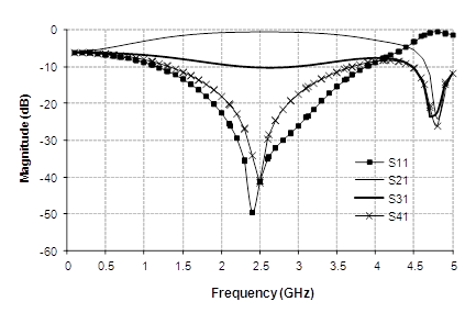
Fig. 6(b). Scattering parameters
The 10-dB loose branch line coupler is designed for the operating frequency 2.5 GHz. From the characteristic response, shown in Fig. 6(b), it is obtained that the coupling from input port to coupled port i.e. from port 1 to port 3 (i.e. S31) is 10 dB at 2.5 GHz. Now, to calculate the fractional band width (FBW) at 10 dB, the characteristic response is re-represented for small frequency span as shown in Fig. 6(c) as follows:
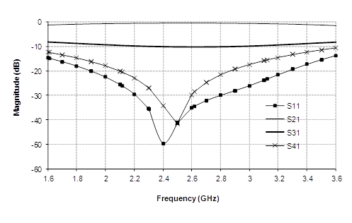
Fig. 6(c). Scattering parameters around center frequency
The above response shows that the structure provides 10 dB coupling from
lower frequency, f1 = 1.9GHz to higher frequency, f2
= 3.2 GHz around center frequency, f0 = 2.5 GHz with
negligible tolerance. Therefore, the fractional bandwidth [FBW= ((f1-f2)/f0)![]() 100%] of the proposed 10-dB branch line
coupler is 52% with zero tolerance.
100%] of the proposed 10-dB branch line
coupler is 52% with zero tolerance.
The following table, Table: 3 shows the FBWs for different considerable tolerances of coupling.
Table: 3FBWs for different considerable tolerances.
|
Tolerance |
|
|
|
|
|
FBW (%) |
52 |
57 |
60.8 |
87.2 |
V. MEASUREMENT AND DISCUSSION
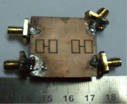
The proposed structure has been fabricated with FR4 substrate. The photonic view of the 10 dB coupler is shown in the following Fig. 7.

(a) (b)
Fig. 7. Photonic Views (a) Top Plane (b) Ground Plane
The proposed 10 dB branch line coupler has been measured with an Agilent make vector network analyzer of model N5230A. The measurement responses of the scattering parameters are shown in the following Figure 8.
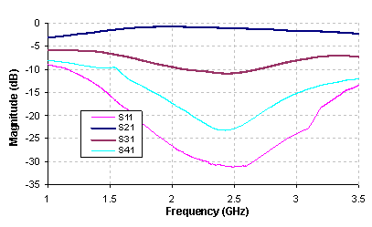
Fig. 8. Scattering Parameters (Measurement responses)
The above responses show that there is a 10.4 dB coupling
between input port and coupled port (S31) at operating frequency 2.5
GHz. Thus, the proposed structure behaves as 10 dB coupler and provides almost
60 % FBW with ![]() 5% tolerance. The different
scattering parameter for simulated and measurement results are shown in Fig. 9.
5% tolerance. The different
scattering parameter for simulated and measurement results are shown in Fig. 9.


(a) (b)
Fig. 9. Scattering Parameters (a) S11 & S31, (b) S21 & S41
From the above analysis with simulated and measurement responses it is observed that the proposed branch line coupler with rectangular ring headed DGS acts as a loose coupler and provides 10dB coupling at the operating frequency 2.5 GHz.
VI. CONCLUSION
Generally, with the help of branch line tight coupler such as 3dB, 6dB etc are designed. In this paper a new concept for designing of loose coupler has been established and as an example one 10-dB branch line coupler is designed. Here, the main branch line is obtained by simple conventional microstrip line and the high impedance shunt branch line is formed by introducing DGS underneath a conventional microstrip line. Adding DGS introduces some inductance and increases the effective electric length of the microstrip line and provides slow-wave characteristics. Finally, one 10-dB branch line coupler is designed, fabricated and measured and there is a good agreement between simulated and measurement results have been obtained. However, though 10-dB branch line coupler is designed by using the proposed concept but utilizing the same concept any loose coupler, such as 15dB, 20 dB etc can easily be obtained.
[1] V. Radisic, Y. Qian, and T. Itoh, "Broadband power amplifier using dielectric photonic bandgap structure," IEEE Microwave Guide Wave Lett. Vol.8, pp.13-14, Jan. 1998.
[2] V. Radisic, Y. Qian, and T. Itoh, "Novel Architectures for high-efficiency amplifiers for wireless applications," IEEE Trans. Microwave Theory and Techniques, Vol.46, No.11, pp.372-374, Nov. 1998.
[3] C. S. Kim, J. S. Park, D. Ahn, and J. B. Lim, "A Novel 1-D Periodic Defected Ground Structure for Planar Circuits," IEEE Microwave and Guided Wave Letters, Vol.10, No.4, pp.13 1-133, April, 2000.
[4] F-R. Yang, Y. Qian, R. Coccioli, and T. Itoh, "A novel low-loss slow wave microstrip structure," IEEE Microwave Guide Wave Lett. Vol.8, No.11, pp.372-374, Nov. 1998.
[5] Y. Qian, F-R.Yang, and Tatsuo Itoh,"Characteristics of microstrip lines on a uniplanar compact PBG ground plane," APMC'98 Proc, pp.589-592, 1998.
[6] J. I. Park, C. S. Kim, J. Kim, J-S Park, Y. Qian, D. Ahn, and T. Itoh, "Modeling of a photonic bandgap and its application for the low-pass filter design," APMC'99, Dig., pp.331-334, Nov. 1999.
[7] C.S. Kim, J.S. Park, D. Ahn, and J.B. Lim, “A novel 1-D periodic defected ground structure for planar circuits,” IEEE Microw. Guid. Wave Lett., vol. 10, no. 4, pp. 131–133, Apr. 2000.
[8] C.-S Kim, J.-S. Lim, D. Ahn and S. Nam, “A 10db branch line coupler using defected ground structure,” EUMC’2000, Dig.,pp. 1-4, Oct. 2000.
[9] Changjiang You* and Xiaowei Zhu, “A Novel Planar Dual-Band Branch Line Coupler Using Defect Ground Structure” IEEE MTT-S International pp. 1227-1230, 2008.
